1State Key Laboratory of Luminescence and Applications, Changchun Institute of Optics, Fine Mechanics and Physics, Chinese Academy of Sciences, Changchun 130033, China
2Center of Materials Science and Optoelectronics Engineering, University of Chinese Academy of Sciences, Beijing 100049, China
3Key Laboratory of Electronic Materials and Devices of Tianjin, School of Electronics and Information Engineering, Hebei University of Technology, Tianjin 300401, China
240 nm AlGaN-based micro-LEDs with different sizes are designed and fabricated. Then, the external quantum efficiency (EQE) and light extraction efficiency (LEE) are systematically investigated by comparing size and edge effects. Here, it is revealed that the peak optical output power increases by 81.83% with the size shrinking from 50.0 to 25.0 μm. Thereinto, the LEE increases by 26.21% and the LEE enhancement mainly comes from the sidewall light extraction. Most notably, transverse-magnetic (TM) mode light intensifies faster as the size shrinks due to the tilted mesa side-wall and Al reflector design. However, when it turns to 12.5 μm sized micro-LEDs, the output power is lower than 25.0 μm sized ones. The underlying mechanism is that even though protected by SiO2 passivation, the edge effect which leads to current leakage and Shockley-Read-Hall (SRH) recombination deteriorates rapidly with the size further shrinking. Moreover, the ratio of the p-contact area to mesa area is much lower, which deteriorates the p-type current spreading at the mesa edge. These findings show a role of thumb for the design of high efficiency micro-LEDs with wavelength below 250 nm, which will pave the way for wide applications of deep ultraviolet (DUV) micro-LEDs.
AlGaN based deep ultraviolet (DUV) LEDs are extensively studied due to their customizable wavelengths, small size, high efficiency, high modulation bandwidth, long lifetime, and friendly to the environment[1−5]. Up to date, DUV LEDs are widely used for non-light-of-sight optical communication, sensing systems, sterilization, and medical phototherapy[6−8]. However, the 280 nm wavelength is harmful to the human eyes and skin. Recent work has shown that shorter wavelengths from 255 to 220 nm can be more effective at sterilization[9], while higher photon energies feature shallower penetration depth for the stratum corneum, which can avoid the deleterious effects of the human beings when exposure to UV light[10, 11]. Similarly, the DUV light for non-line-of-sight communications always travels through the air and shorter wavelengths can protect human beings from damage by DUV light. Moreover, micro-LEDs have higher modulation bandwidth, which is essential for non-line-of-sight communications. Micro-LEDs can also be combined with face recognition technology and programmed to keep away from human faces during sterilization and disinfection. Given these promising applications, the 240 nm AlGaN-based micro-LEDs are grown and fabricated.
The flip-chip structured micro-LEDs always have a current crowding effect at the mesa edge, which leads to self-heating and uneven current distribution[12, 13]. This current crowding effect derives from the flip-chip structure. As p-type current spreading is solved by the metalized current spreading layer, the n-type current spreading length is limited by the relative high n-AlGaN resistivity, which leads to the electrons crowded at the mesa edge. To address this issue, Martin Dawson’s group studied the size effect of micro-LEDs and found that smaller sized micro-LEDs can relieve the self-heating and enhance the modulation bandwidth[14, 15]. Sun et al. enhanced the optical performance of deep ultraviolet micro-LEDs through the perimeter-to-area ratio engineering[16]. Demir’s group put forward the effective n-electrode length model and found that mini-LEDs with longer effective n-electrode length show lower self-heating and higher output optical power[12]. Long et al. demonstrated that smaller chip sizes can reduce the current crowding induced self-heating effect[17].
However, for n-AlGaN with high Al composition, the resistance is higher as the n-type doping concentration is lower. This high resistance contributes to much shorter n-type current spreading length for DUV LEDs than that in conventional GaN-based visible LEDs, and results in even higher current crowding and self-heating[13, 18]. This severe self-heating caused by the low power conversion efficiency of DUV LEDs is mainly responsible for the considerable decrease of efficiency when current crowding is present[13]. Therefore, it is essential to systematically study how to reduce the current crowding effect for 240 AlGaN-based micro-LEDs.
2. Theoretical consideration of the device design
To find the possible solutions for the severe current crowding, we calculated the current density distribution based on the current spreading model in Fig. 1(a). The results show that this high n-type resistance may also cause severe nonradiative recombination and current leakage at the mesa edge. The details are as follows:
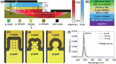
Figure 1.(Color online) (a) Schematic diagram of the current distribution for the flip-chip structured micro-LEDs. (b) Schematic illustration of the epitaxial layers. Different sized micro-LEDs: R = (c) 12.5 μm, (d) 25.0 μm, and (e) 50.0 μm. (f) Spectrum of 12.5 μm sized micro-LEDs under various currents.
Here, stands for voltage drop across metal semiconductor contact barrier for both p-&n-contact, stands for voltage drop across pn junction, stands for voltage drop across p-GaN and p-AlGaN, and stands for voltage drop across n-AlGaN. Based on Shockley equation, can be expressed as
Here, k is Boltzmann constant, T is the temperature, J is the current density, J0 is the reverse saturation current density, and e stands for elementary charge. At high forward current density area, Vpn changes slightly with J changing. At position , for a small distance , as changes slightly at high forward current area, the current is:
Here, and stands for resistance of p-GaN and p-AlGaN across the thickness of tp, and n-AlGaN across the distance of x along x-axis, respectively, as shown in Fig. 1(a). For a certain distance , we can get is constant. is the resistivity of n-AlGaN, and is the cross-section area of n-AlGaN along direction. From Eq. (1), for a certain and , as is nearly constant, is also nearly constant. From Eq. (3), as , , , and is nearly constant, we can conclude that decreases as increases, and decreases faster when is larger. Similarly, the hole density will also decrease from the p-contact edge, which closes to mesa edge, as exhibited in Fig. 1. Hence, at area A, is the highest, and is the highest. As and is the thickness of p-GaN and p-AlGaN, which is constant, the electric field is the highest at area A. The electric filed will drive the holes into the multiple quantum wells (MQWs), and similarly for the electrons. Therefore, the holes and electrons will be the highest at area A, which results in severe current leakage and nonradiative recombination. If the mesa is surrounded by n-electrode instead of at one side of the mesa, the total length of area A perpendicular to the figure plane is longer and the current density in area A can be reduced. As the circular mesa disk has the longest perimeter for a certain mesa area, we designed circular shaped micro-LEDs to relieve the current crowding of the micro-LEDs, as shown in Fig. 1(d). Moreover, through calculation, we find that smaller sized micro-LEDs possess longer total mesa perimeter, which can further reduce the current crowding in area A. However, as the mesa edge is close to or in area A, the current leakage and nonradiative recombination rate is high because of the edge effect. In addition to the size effect, the edge effect should also be taken into consideration. Therefore, we designed and fabricated different sized micro-LEDs, as illustrated in Figs. 1(c)−1(e). Then the optical and electrical properties are systematically studied.
3. Experiment and numerical simulation details
The AlGaN-based micro-LED epitaxial layers were grown on a 2-inch high temperature annealed AlN/sapphire template by our high-temperature metal−organic chemical vapour deposition (HT-MOCVD) system, as shown in Fig. 1(b). Firstly, a few periods of AlN/AlGaN superlattices were prepared, then followed a 1.2 μm thick Si-doped Al0.8Ga0.2N electron injection layer and five pairs of Al0.7Ga0.3N/Al0.85Ga0.15N multiple quantum wells (MQWs), next was a Mg-doped p-Al0.8Ga0.2N layer, and finally a p-GaN layer was grown. The epi-wafers were subsequently processed into micro-LED chips by a standard microfabrication process. These micro-LEDs were designed in three sizes but all have the same total device mesa area: a 4 × 4 micro-LED matrix with a mesa radius of 12.5 μm, a 2 × 2 micro-LED matrix with a mesa radius of 25.0 μm, and a 1 × 1 micro-LED matrix with a mesa radius of 50.0 μm. The mesa was prepared by using inductively coupled plasma (ICP) etching. The mesa side-walls were protected by a layer of 1.2 μm SiO2, which acts as a passivation layer to reduce the nonradiative recombination and current leakage. To enhance the light extraction efficiency (LEE), the mesa sidewall was etched 30° to the wafer plane as this angle contributes to the higher LEE based on previous study[19−22]. Ti/Al based metal layers, annealed at 600 °C in N2 ambient for 3 min, were used as n-contacts. Ni/Al alloys annealed at 500 °C in N2 ambient for 3 min were used as p-type current spreading layers. Here, we keep a 5 μm margin between the p-contact edge and the mesa edge for all the different sized micro-LEDs. To further enhance the LEE, an Al overlay reflector was placed on the top of SiO2. Ti/Al/Ti/Au multi-layers were used as p-&n-pad, where Al is 1.3 μm to reflect light from chip side-walls for light extraction. After fabrication, the optical output power is measured by an integrating sphere. The I−V characteristics of different sized micro-LEDs are carried out by Keithley semiconductor analyzer.
To further investigate the underlying physics, numerical simulations were carried out by APSYS, where various mathematical equations including Schrödinger equation, Poisson’s equation and drift-diffusion equation, etc. are self-consistently handled. The auger recombination coefficient was set to 10−30 cm6/s[23]. The Shockley-Read-Hall (SRH) lifetimes were set to 2 × 10⁻⁸, 1 × 10⁻⁸, and 5 × 10⁻⁹ s for 50.0, 25.0, and 12.5 μm sized micro-LEDs, respectively[24−26]. The polarization level and the band offset between AlGaN/AlGaN heterojunction materials were set to 40% and 50 : 50[27, 28], respectively. The LEEs for different sized micro-LEDs were calculated by utilizing the finite different time domain (FDTD) method[29]. Then the calculated LEEs were taken into consideration for the APSYS numerical simulation results. Other parameters on AlGaN-based semiconductors can be found elsewhere[30].
4. Results and discussion
Table 1 shows the LEE results for different sized micro-LEDs based on FDTD numerical simulations. From Table 1 we can observe that with the size shrinking, the LEEs for both the transverse-magnetic (TM) polarized light and the transverse-electric (TE) polarized light are enhanced. What is noteworthy is that the LEE of TM-mode light increases faster than that of TE-mode light. This happens because we etched tilted mesa side-walls for these micro-LEDs and these tilted side-walls enhance TM-mode light more efficiently than TE-mode light. In addition, there are more side-walls for smaller sized micro-LEDs.
To further investigate the underlying reasons of the LEE variation depends on the micro-LED size, the electric field distributions of the TE-&TM-polarized light for different sized micro-LEDs are analyzed by using Lumerical FDTD solution. Figs. 2(a) and 2(b) are the SEM images of 12.5 μm sized micro-LED to show the mesa side-wall slant angle. From Fig. 2(b) we can see that the side-wall is inclined at an angle of 30°. This tapered angle contributes to the side-wall light extraction, especially for TM-mode light extraction as depicted in the inset figure within Fig. 2(b). The FDTD simulation model for different sized micro-LEDs is illustrated in Fig. 2(c). The dipole source polarization direction was set parallel to the Y-axis for TM-mode light or parallel to the X-axis for TE-mode light. The mesa side-wall tilt angle was set 30° to the wafer plane as this angle contributes to higher LEE based on previous study[21, 22]. Other parameters can be found elsewhere[20, 29]. Figs. 2(d)−2(f) stand for the electric field distribution of TE-mode light for R = 50.0, 25.0, and 12.5 μm sized micro-LEDs, respectively. From Figs. 2(d)−2(f) we can observe that the light mainly extracted from the mesa centers, next from the tilted side-walls between two mesas, and finally from the chip edges. As the size decreases from 50.0 to 12.5 μm, the numbers of the mesa centers and side-walls increase rapidly, which results in more light extraction centers and finally enhances the LEE for smaller sized micro-LEDs. Figs. 2(g)−2(i) stand for TM-mode light distribution of FDTD results for R = 50.0, 25.0, and 12.5 μm sized micro-LEDs, respectively. From Figs. 2(g)−2(i), we can see that different from TE-mode light, TM-mode light mainly extracted from the tilted side-walls between two mesas, next from the mesa centers and chip edges. The reason is that as TM-mode light mainly travels horizontally, the side-wall light extraction dominates, and less light is extracted from the backside of the chip. This is also the main reason why LEE of TM-mode light increases faster with the size decreasing, most notably the 12.5 μm size, for which the LEE of TM is higher than that of TE as the side-wall length is the longest among them. For the LEE difference of TE part and TM part for the 50.0 μm sized micro-LEDs, as this size has less side-wall length for TM-mode light extraction, the TE part of the LEE is higher than TM part, as can be compared by Figs. 2(d) and 2(g). Therefore, the LEE enhancement is mainly from the side-wall light extraction both for TE and TM-mode light with the size shrinking, most notably TM-mode light enhancing faster for this 30° side-wall angle.
Table Infomation Is Not Enable
Figure 2.(Color online) SEM images of 12.5 μm size micro-LED (a) mesa and (b) cross section of the side-wall tilt angle. The inset within (b) is the schematic diagram of micro-LED 30° tilted side-wall light extraction. (c) Schematic diagram of 2D-FDTD simulation model for different sized micro-LEDs. Electric field distributions in the XY cross section of the TE-polarized light for (d) R = 50.0 μm , (e) 25.0 μm, and (f) 12.5 μm sized micro-LEDs, and TM-polarized light for (g) R = 50.0 μm , (h) 25.0 μm , and (i) 12.5 μm sized micro-LEDs.
To verify whether the aforementioned conclusion is suitable for different angles, we further studied the LEE changes depending on the micro-LED sizes and mesa side-wall angles, as shown in Fig. 3. From Fig. 3(a) we can observe that with the size shrinking the LEE for the TE-polarized light (LEE-TE) is enhanced for both 45° and 30°. However, for 60°, the LEE-TE is nearly the same for different sized micro-LEDs. For 75°, the LEE-TE is reduced with the size shrinking. Therefore, the side-wall only contributes to the LEE-TE with small angles. From Fig. 3(b) we can observe that with the size shrinking, the LEE for the TM-polarized light (LEE-TM) is enhanced for all the simulated angles. Comparing Fig. 3(a) with 3(b), we can find that with the size shrinking LEE-TM enhancing is much better than LEE-TE for all the simulated angles.
Figure 3.(Color online) (a) LEE-TE and (b) LEE-TM for different sized micro-LEDs based on FDTD numerical simulations.
After the LEE, we further studied the optical characteristics of different sized micro-LEDs. Fig. 4 shows the optical output power and EQE as a function of the current for various sized micro-LEDs. Here, the LEE is carefully considered in the numerical simulation results in Fig. 4(b). We adopted the same intensity of the TM part and TE part for the 240 nm wavelength based on the optical light polarization study of Guttmann et al.[31]. From Figs. 4(a) and 4(b), we can observe that the numerical simulation results match well with the experimental results. With the size decreasing from 50.0 to 25.0 μm, the peak optical output power based on the experimental data increases 81.83%. One of the reasons is that the LEE enhances 26.21% with the size shrinking. Another reason is the aforementioned current density distribution uniformity property. To further explore the possible electrical reasons for the characteristics of the output power, numerical simulations are conducted. The current density distributions along the MQWs are shown in Figs. 5(a)−5(d). Comparing Figs. 5(a) and 5(b), we can find that the current density uniformity of 25.0 μm sized micro-LEDs is much better than that of the 50.0 μm sized ones. This uniform current density also suppresses self-heating and benefits the internal quantum efficiency (IQE). Fig. 5(e) is the wavelength as a function of the current for different sized micro-LEDs. As the current increases, the wavelength blue-shifts first due to quantum-confined Stark effect (QCSE) screening and band filling by injected carriers[32], and then the wavelength red-shifts because of the increased junction temperature[33]. Moreover, the wavelength red-shifts further as the temperature rises. Hence, the wavelength red-shift can be used to compare the junction temperature. From Fig. 5(e), it is obvious that the wavelength of 50.0 μm sized micro-LEDs red-shift more than that of the 25.0 μm sized ones, indicating that 50.0 μm sized micro-LEDs have a higher junction temperature. This high junction temperature will further restrain the IQE and output power at high current level. Therefore, the lower LEE, current density nonuniformity, and self-heating are the main factors for the lower optical output power for the 50.0 μm sized micro-LEDs.
Figure 4.(Color online) Optical output power and EQE for various sized micro-LEDs: (a) experimental results and (b) numerical simulation results.
Figure 5.(Color online) Apsys simulation results of current density distribution along the MQWs for (a) 50.0 μm, (b) 25.0 μm, and (c)&(d) 12.5 μm sized micro-LEDs based on the model of Fig. 1(a). Here, compared to (c), (d) is closer to the n-electrode. (e) Wavelength−current relationship for different sized micro-LEDs.
However, even though the LEE is enhanced, the output power for 12.5 μm sized micro-LEDs is lower than that of the 25.0 μm sized ones, as illustrated in Fig. 4. These results are different from the individual devices, for which the smaller size has higher optical output power density[17]. This happens because the smaller individual device generates less total heat and its heat dissipation sink is relatively bigger. With regard to our devices, as the different sized micro-LEDs are fabricated on the same wafer, the only differences are the mesa size, the mesa side-wall lengths, and the p-contact areas. Hence, we analysis the optical performance from three aspects. Firstly, the edge effect depends on the mesa perimeter. From Table 2 we can observe that the mesa perimeter of 12.5 μm sized micro-LEDs is twice that of the 25.0 μm sized ones, and that of the 25.0 μm sized ones is also twice that of the 50.0 μm sized ones. As well known, the mesa side-wall always leads to edge effect, which results in current leakage and SRH recombination. From the inset in Fig. 6, we can see that the 12.5 μm sized micro-LED shows the highest leakage current, which corresponds to the shortest SRH lifetime. The 50.0 μm sized micro-LED shows the lowest leakage current, which corresponds to the longest SRH lifetime. The SRH lifetime is typically set to 10−8 s level[34, 35]. Hence, we set the SRH lifetime for the 50.0 μm sized micro-LEDs to 2 × 10⁻⁸ s, the 25.0 μm sized ones to 1×10⁻⁸ s, and 12.5 μm sized ones to 5 × 10⁻⁹ s in the numerical simulations. However, the SRH values are complex and not easy to estimate, so the SRH lifetimes are not the real values. Here, the SRH lifetime is just used to estimate the size effect based on the previous study method[36]. Secondly, besides the edge effect, the total p-contact area difference due to the size effect also affects the output power. From Table 2, it is obvious that the ratio of total p-contact area to the mesa area for 12.5 μm sized micro-LEDs is much smaller than that of either 25.0 μm sized ones or 50.0 μm sized ones. This much smaller ratio will lead to current nonuniformity and lower light reflection, which result in lower LEE and output power for the 12.5 μm sized micro-LEDs[37]. From Fig. 5(d), it is clearly that the current density reduces dramatically at the mesa edge margin area without p-contact. Thirdly, as the distances to the n-electrode are different for the 12.5 μm sized micro-LED mesa disks, there is an impressive current density difference for these two types of mesa disks, as illustrated in Figs. 5(c) and 5(d). This results in unevenness of current density for the 12.5 μm sized micro-LEDs and further leads to lower IQE and output power. Therefore, even though the LEE of 12.5 μm sized micro-LEDs is higher than that of the 25.0 μm sized ones, because of the severe edge effect due to longer side-walls, much smaller ratio of p-contact area to mesa area, and nonuniformity of current density on account of different n-electrode distances, the optical output power of the 12.5 μm sized micro-LEDs is lower than that of the 25.0 μm sized ones.
Figure 6.(Color online) The current−voltage characteristics of different sized micro-LEDs: (a) experimental results, (b) numerical simulation results.
We also studied the current-voltage characteristics for different sized micro-LEDs, as depicted in Fig. 6. It is worth note that the turn-on voltage is high. The underlying reason is that the 240 nm DUV LED needs high Al incorporation, which leads to lower doping efficiency. This low hole and electron concentration contributes to higher contact resistance and results in high voltage for these 240 nm micro-LEDs. However, this high turn-on voltage will result in device reliability issue. Therefore, its voltage property needs to be optimized in the future research work. Nevertheless, the trend of the I−V characteristics can still be used to reflect the underlying physics. From Fig. 6, it exhibits that at the same current, the voltage decreases as the size shrinks. It is worth noting that the reverse current at −5 V for the 12.5 μm sized micro-LEDs is much higher than that of either 25.0 μm sized ones or 50.0 μm sized ones, as shown in the inset within Fig. 6(a). The underlying reasons are that the 12.5 μm sized micro-LEDs have the longest mesa side-wall perimeter, as exhibited in Table 2 and higher current density at the mesa edge than the 50.0 μm sized ones, as illustrated in Figs. 5(b) and 5(d). This further clarifies the serious edge effect of the 12.5 μm sized micro-LEDs.
5. Conclusions
In summary, 240 nm AlGaN based micro-LEDs are grown and fabricated. Based on FDTD study, we found that the LEE increases with the size decreasing. The tilted side-wall and Al overlay are the main factors that boost the light extraction efficiency of the smaller sized micro-LEDs. It is worth noting that the LEE of TM-mode light enhancing faster with the size shrinking and LEE of TM-mode light is higher than that of TE-mode light for the 12.5 μm micro-LEDs. This is important for the LEDs with wavelength shorter than 240 nm, for which TM-mode light dominates. On the other hand, the total mesa perimeter is also increasing with the size getting smaller, which alleviates the current crowding and self-heating. Hence, the optical output power of 25.0 μm sized micro-LEDs is higher than that of the 50.0 μm sized ones. However, the longer mesa perimeter is a double-edged sword. The 12.5 μm sized micro-LEDs suffer from severe edge effect and results in lower IQE because of this too long mesa perimeter. However, if the side-wall is further protected, such as being treated by KOH and ALD Al2O3 instead of SiO2 that we used, the 12.5 μm sized micro-LEDs may have high promising performance. Moreover, the much lower ratio of the p-contact area to the mesa area is another essential factor that leads to nonuniformity current density and reduced IQE of the 12.5 μm sized micro-LEDs. Apart from that, the longer distance of the centered mesa disk to the n-electrode is another factor for the uneven current density of the 12.5 μm sized micro-LEDs. Because of these unfavorable factors, the output power of the 12.5 μm sized micro-LEDs is lower than that of the 25.0 μm sized ones. Therefore, based on our fabrication process, the 25.0 μm sized micro-LEDs possess the highest optical output power.
[33] S Chhajed, Y Xi, T Gessmann et al. Junction temperature in light-emitting diodes assessed by different methods. Integrated Optoelectronic Devices 2005 (SPIE, 2005), 5739(2005).