• Acta Optica Sinica
  • Vol. 38, Issue 5, 0514001 (2018)
Zhaochen Lü1, Qing Wang、*, Shun Yao1, Guangzheng Zhou1, Hongyan Yu1, Ying Li1, Luguang Lang1, Tian Lan1, Wenjia Zhang1, Chenyu Liang1, Yang Zhang1, Fengchun Zhao1, Haifeng Jia1, Guanghui Wang1, and Zhiyong Wang1
Author Affiliations
  • 1 Institute of Laser Engineering, Beijing University of Technology, Beijing 100124, China
  • 1 National Key Laboratory of Regional Fiber Communication Network and New Optical Communication System, Shanghai Jiao Tong University, Shanghai 200030, China
  • 1 Sino Semicondutor Photonic Integrated Circuit Co., Ltd., Taizhou, Jiangsu 225300, China
  • show less
    DOI: 10.3788/AOS201838.0514001 Cite this Article Set citation alerts
    Zhaochen Lü, Qing Wang, Shun Yao, Guangzheng Zhou, Hongyan Yu, Ying Li, Luguang Lang, Tian Lan, Wenjia Zhang, Chenyu Liang, Yang Zhang, Fengchun Zhao, Haifeng Jia, Guanghui Wang, Zhiyong Wang. 4×15 Gbit/s 850 nm Vertical Cavity Surface Emitting Laser Array[J]. Acta Optica Sinica, 2018, 38(5): 0514001 Copy Citation Text show less
    Schematic of 850 nm VCSEL structure
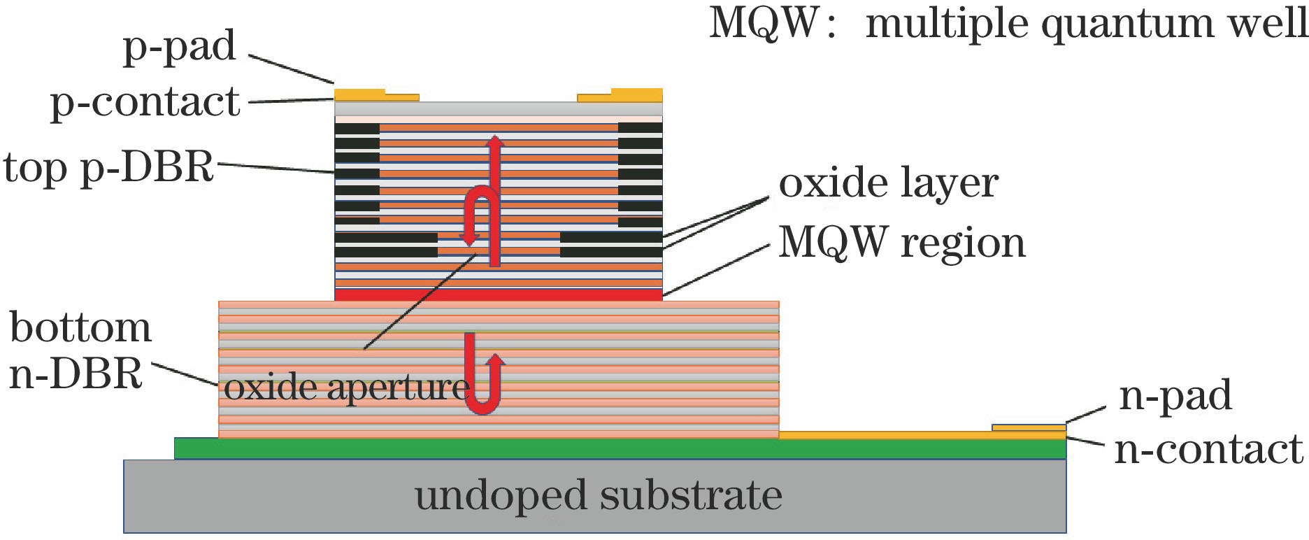
    Fig. 1. Schematic of 850 nm VCSEL structure
    (a) PL spectrum of active region at 25 ℃; (b) white light reflection spectrum of VCSEL
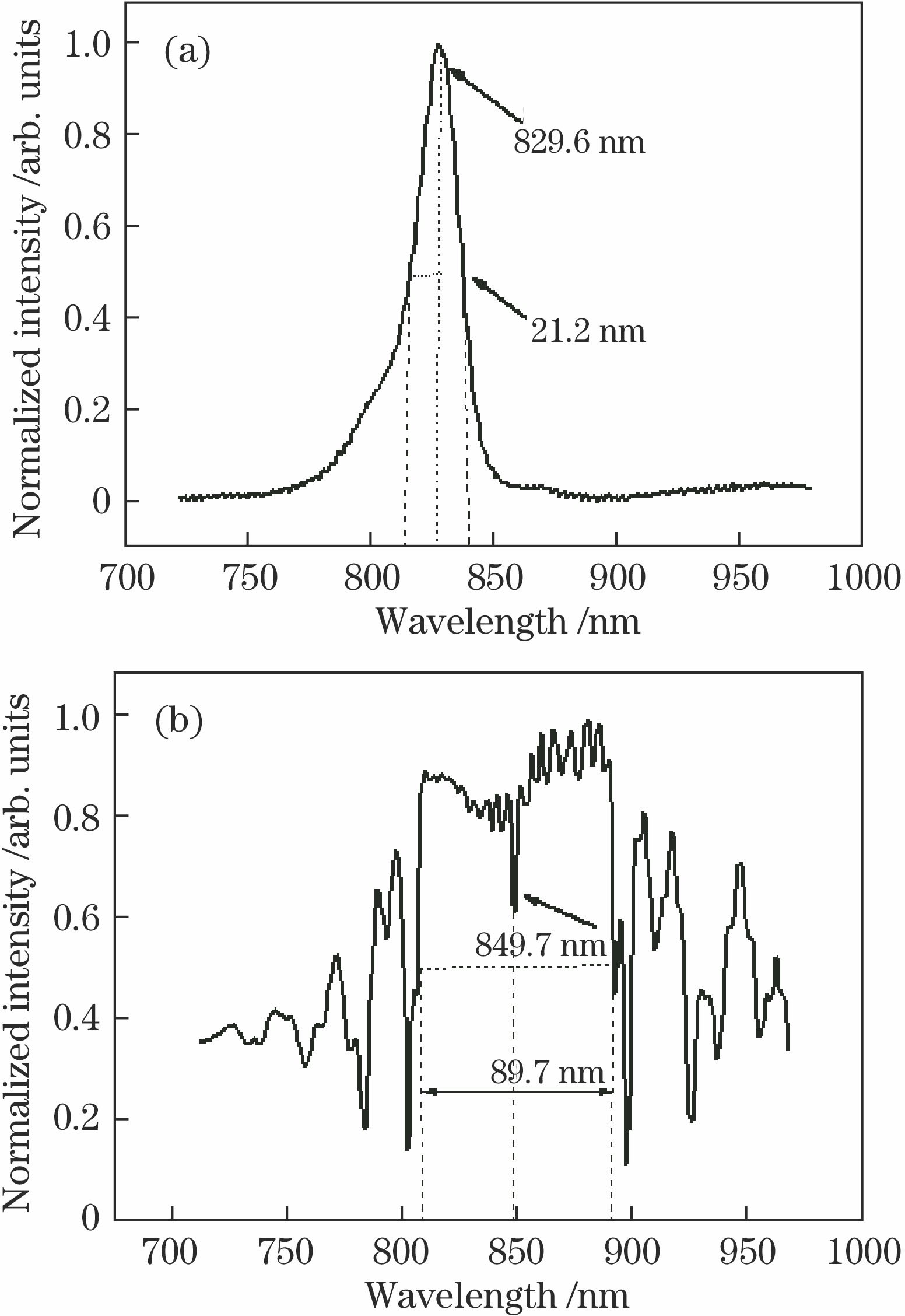
    Fig. 2. (a) PL spectrum of active region at 25 ℃; (b) white light reflection spectrum of VCSEL
    (a) Grid cells on the mask; (b) arrangement of chips in the grid cells; (c) oxidation aperture distribution in each cell on the wafer under the infrared light source CCD; (d) size of oxidation aperture on each cell of the wafer
    Fig. 3. (a) Grid cells on the mask; (b) arrangement of chips in the grid cells; (c) oxidation aperture distribution in each cell on the wafer under the infrared light source CCD; (d) size of oxidation aperture on each cell of the wafer
    Images of 1×4 VCSEL array
    Fig. 4. Images of 1×4 VCSEL array
    (a) P-I-V curves of 1×4 VCSEL array; (b) spectrum of VCSEL
    Fig. 5. (a) P-I-V curves of 1×4 VCSEL array; (b) spectrum of VCSEL
    Far field spot and divergence angle of single VCSEL
    Fig. 6. Far field spot and divergence angle of single VCSEL
    (a) Box diagram of VCSEL threshold current; (b) box diagram of VCSEL optical output power at driving current of 6 mA; (c) box diagram of VCSEL wavelength at driving current of 6 mA
    Fig. 7. (a) Box diagram of VCSEL threshold current; (b) box diagram of VCSEL optical output power at driving current of 6 mA; (c) box diagram of VCSEL wavelength at driving current of 6 mA
    High-speed test platform with pulse large signal
    Fig. 8. High-speed test platform with pulse large signal
    Four-channel optical eye diagrams after signal with modulation rate of 15 Gbit/s transmission in multimode fiber for 1.5 m. (a) P1 channel; (b) P2 channel; (c) P3 channel; (d) P4 channel
    Fig. 9. Four-channel optical eye diagrams after signal with modulation rate of 15 Gbit/s transmission in multimode fiber for 1.5 m. (a) P1 channel; (b) P2 channel; (c) P3 channel; (d) P4 channel
    Wafer positionUpperBottomMiddleLeftRight
    Etching depth /nm3625.43607.73577.83645.43699.8
    Table 1. Etching depth of different positions of first mesa in VCSEL
    Zhaochen Lü, Qing Wang, Shun Yao, Guangzheng Zhou, Hongyan Yu, Ying Li, Luguang Lang, Tian Lan, Wenjia Zhang, Chenyu Liang, Yang Zhang, Fengchun Zhao, Haifeng Jia, Guanghui Wang, Zhiyong Wang. 4×15 Gbit/s 850 nm Vertical Cavity Surface Emitting Laser Array[J]. Acta Optica Sinica, 2018, 38(5): 0514001
    Download Citation