
Thomas Hirtz, Steyn Huurman, He Tian, Yi Yang, Tian-Ling Ren. Framework for TCAD augmented machine learning on multi- I–V characteristics using convolutional neural network and multiprocessing[J]. Journal of Semiconductors, 2021, 42(12): 124101
- Journal of Semiconductors
- Vol. 42, Issue 12, 124101 (2021)
Abstract
1. Introduction
Machine learning and data science are revolutionizing many domains with techniques that manipulate data and exploit useful information and patterns. In recent years and among all the computer science subdomains, the fields that have encountered some of the most significant advances (e.g., computer vision and natural language processing) have one common aspect: the ease for researchers and even amateurs to access training data. This allows people to try various new architectures, ideas, or implementations, and it acts as a catalyst for the development of the concerned field. However, in the case of microelectronics, one can hardly find any datasets on free repositories—the data is generally sparse or non-existent. This situation creates a barrier that prevents the field's development in comparison to other domains.
In response, this work will first introduce a technique to create datasets related to semiconductor devices (Section 2). We will then present two distinct approaches to use deep learning with the aforementioned data (Section 3). Finally, we will present the performance of our framework and will give some specific examples of applications (Section 4).
We included these algorithms for two main reasons. First, the implementation enables us to showcase that the generation of the data is effective and can be used in practical applications. Second, these algorithms provide examples of ways to utilize such datasets and they give the reader all of the building blocks that are necessary to undertake more complex projects.
The first example will show how the original device parameters can be found back by looking at the simulated electrical characteristics. This way of handling the data—from characteristics to parameters—could be beneficial in use cases, such as process monitoring or fault detection.
In the second example, we explain how the simulation parameters can be used to directly predict the results of a simulation. This allows us to simulate all of the devices at more than 9000 times normal speed within the training range and can be applied widely. Examples of these applications include compact modeling, design optimization, and device design.
While machine learning and TCAD simulations have been paired before, most of the work that was previously presented is generally used for specific use cases. Meanwhile, few studies have managed to obtain good results using deep learning techniques.
In 2019, Bankapalli et al. proposed a technique that uses machine learning to reverse engineer devices[
Besides the previously mentioned papers, works that combine device data and machine learning generally focus on compact models[
In our work, we present a widely generalizable method that can both reverse engineer the device and generate new devices. It does not require extremely rigorous preprocessing, besides data standardization and log transformation. Moreover, we applied convolutional neural network techniques on multi I–V curves, which takes all the characteristics of the device as a whole. By not doing dimensionality reduction, such as figures of merit analysis or PCA analysis, we allow the model to know all of the details of the devices and gain precision.
2. Data generation
This first section will present how to build a dataset. It is structured in three parts. Subsection 2.1 will explain how individual devices are simulated. Subsection 2.2 presents the process for simulating multiple devices. Finally, we tackle efficiency and scalability in Subsection 2.3. The whole data generation process is illustrated in Fig. 1(a).
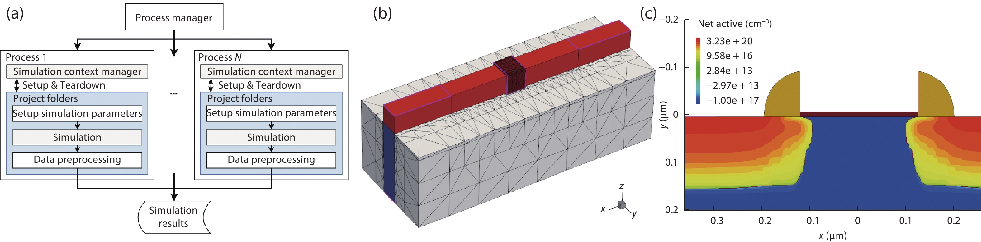
![]()
Figure 1.(Color online) (a) Diagram representing the workflow of generating the training samples. The simulations are distributed among workers using multiprocessing. Those workers are assigned to the different cores of the CPU and executed concurrently. (b) Structure of a FinFET used for the research. The tunable device parameters, along with their values, are: channel doping concentration (1017 cm–3), gate oxidation thickness (1 nm), and SD doping concentration (8 × 1019 cm–3). (c) Structure of the default NMOS used for the research. The process parameters that can be tuned as well as their default values are: N-well concentration (1017 cm–2), gate oxidation time (10 min), LDD dose (1014 cm–2) and LDD energy (30 keV).
2.1. Device simulation
Simulation data can be generated by making use of the software Sentaurus technology computer-aided design (TCAD). To demonstrate the generalizability of the method, we chose to use two different combinations of devices and simulation methods: 3D FinFETs using a structure editor[
For each device, before a simulation, a value combination of simulation parameters needs to be set. These parameters will be the “labels” of our sample. Meanwhile, the “datum” of our sample will be the simulated device measurements. For our transistors, we chose to use value combinations of one to seven distinct simulation parameters, while up to five distinct electrical characteristics were simulated. Figs. 1(b) and 1(c) shows examples of simulated transistors; its caption enumerates several possible device parameters. Moreover, some examples of simulated curves are given in Fig. 2, along with their name in the description.
![]()
Figure 2.(Color online) Samples of a training dataset using planar NMOS. Each line represents one curve of a training sample. Five distinct NMOS characteristics are simulated and used: (a)
The devices presented in this paper may not be realistic and may differ from devices encountered in labs or in the industry. This is especially true for shorter gate length devices and state-of-the-art FinFETs possessing models that need to be refined and further tuned with experimental data. However, one of the main goals of this paper is to provide a framework to generate the samples that are required to develop more complicated machine learning related techniques and design performant models. Moreover, the simulation can be adapted to one's needs.
In addition to the process parameters, it is important to note that it is also possible to input material parameters and simulation parameters when generating the dataset. This type of dataset can be used in applications such as simulation calibration.
2.2. Process for a large number of simulations
To efficiently create, run, and save simulations, Sentaurus was wrapped in a Python program. This enables the automatic management of project directories, as well as the performing of preprocessing and other tasks.
A project folder was used as the source for all of the simulations. Instead of exact simulation values, this project contains placeholders for all the specifiable values. Before a new simulation begins, this folder is duplicated using a context manager. Thereafter, all of the placeholders are filled in with a uniform, log-uniform, or normal probability distribution. Each simulation parameter needs to have its own statistical distribution parameters because each simulation parameter can vary in sensitivity (e.g., gate oxidation time is more sensitive than the lightly doped drain (LDD) dose). Each statistical distribution has its own features and advantages: normal distributions can mimic how the parameters are distributed in real experiments, which can be useful for generating defect detection algorithms; uniform distributions allow us to easily implement mappings between simulation parameters and device characteristics; while log-uniform allows us to efficiently map a broader range of the device parameters. To avoid convergence issues and extreme values, a truncated version of the normal distribution was used.
It is worth mentioning here that because the simulation time was the main bottleneck of the project, we tried to use geometrical methods to optimize the sampling method[
After setting up the parameters, the simulation is started by launching the Sentaurus scheduler using Python. When the simulation is finished, the results are extracted from the different files and inserted into the databases. Finally, the used project folder can be deleted.
2.3. From a single process to multiprocessing
Although looping the previously mentioned procedure is sufficient, generating thousands of training samples can become exceedingly slow if the simulated device is complex or if only low computing resources are available. To address this issue, it is possible to use multiprocessing to run several simulations simultaneously. Following Amdahl's law[
3. Applying machine learning to the dataset
In machine learning, neural networks are used to map certain inputs to outputs (i.e., to predict an output based on a certain input). This is done by giving the neural networks a large collection of examples from which they can learn to distinguish patterns. This section will present two distinct practical examples using this paradigm in combination with the generated datasets from Section 2.
The first algorithm predicts the simulation parameters of devices solely based on their electrical characterization. The second example algorithm will use neural networks to map the simulation parameters to the electrical characteristics. In both cases, the parameters will be represented as a 1-dimensional (1D) tensor with each element being a specific process parameter, such as oxidation time or doping concentration. The characteristics are represented as a 2-dimensional (2D) tensor where each channel (the first dimension) represents one of the electrical characteristics and each element in a channel (the second dimension) stores a different data point of this characteristic.
Since both the parameters and the characteristics can assume a wide range of values, standardization was required to prevent a) the loss related to the biggest output overtaking the loss of the smaller outputs, and that b) the convergence of the system would take an extensive amount of time. The mean and standard deviation for the normalization and denormalization were computed solely using the training dataset.
In addition to the fact that values can greatly differ from characteristic to characteristic, a wide range of values can also occur from sample to sample and even within the same sample (e.g., an on-to-off current ratio can reach 1010). For both example algorithms, we use the logarithm function to mitigate this effect. In the first case, we will engineer features by taking the logarithm of the different inputs. Moreover, in both cases, we will predict the logarithm of the target and apply an exponential function afterwards to find back the true target.
To apply this transformation, we utilize normalization and de-normalization layers. This architecture with two outputs allows us to train our neural networks using normalized data while directly outputting the data possessing the right scale. The loss takes three inputs: the normalization parameters, the true value, and the predicted normalized value. The right conversions are done internally and seamlessly. The details of the architectures are available on Fig. 3(a) and Fig. 4(a).
![]()
Figure 3.(Color online) (a) Neural network architecture used for mapping the characteristics of a device to the process parameters. The 13 input channels are composed of the five current characteristics, the voltage of the off-state breakdown curve (when simulating the breakdown curve, the current is set and the voltage is therefore variable, in contrast to the other voltage characteristics), their logarithmic counterpart as well as the index values. (b) Scatter plots representing the values predicted by the network (
![]()
Figure 4.(Color online) (a) Neural network architecture used for mapping the process or device parameters to its electrical characteristics. (b) Training curves for the predictions of characteristics using different numbers of training samples.
The two algorithms were implemented using TensorFlow. The number of samples is quite limited (between 3000 and 20 000 samples) in comparison to classical applications of deep learning. Therefore, the different networks were designed to use fewer trainable parameters to prevent overfitting and provide a better generalization.
All of the graphs that are presented in this paper that display predictions of the network (Fig. 5), or the actual values versus the predictions (Fig. 3(b) or Fig. 5), use neural networks that are trained with 3000 samples and tested with 1000 previously unseen samples.
![]()
Figure 5.(Color online) (a) Plots representing NMOS characteristics predicted by the network (solid line) versus the actual values (dotted line) of three samples from the validation dataset. The samples were not previously seen by the network. (b) Prediction of characteristics with three parameters fixed and the N-well concentration spread evenly over its range of value. The gate oxidation time, LDD Dose and LDD Energy are set at 12.5 min,
Note that the following sections discuss the use of higher-dimensional data used as input or output of neural networks. If the figures of merit (e.g. subthreshold swing) are the device properties that need to be studied, then it is possible to train lighter models that directly predict them using devices’ parameters.
3.1. Prediction of the simulation parameters
The principle of the first algorithm’s implementation is to extract features from the characteristics to predict the simulation parameters.
The architecture that we used, as shown in Fig. 3(a), resembles the LeNet-4[
Fig. 3(b) display the prediction of all the datapoint present in the test set. None of the devices present in the test set were previously seen by the network. The x-axis represents the true value of the parameter, while the y-axis represents the prediction done by the network. The predictions are better when the points are closer to the x = y line. We can see that the network can reverse engineer the device parameters with very high fidelity using the electrical characteristics.
To quantify the performance of our network, we computed the R2 values for each device parameter. The R2 explains the correlation between the actual value and the predicted value. It measures the degree to which the independent variables explain the dependent variable. In our case, the feed-forward network allows us to explain between 99.9% and 98.2% of the variation of the parameters of our FinFET using electrical characteristics.
Note that the more a parameter influences the electrical characteristics of the device, the easier it is to predict this parameter using the aforementioned characteristics. In the FinFET case, the gate thickness and the SD doping concentration are the parameters that have the most influence on the device.
3.2. Prediction of the characteristics
With the second algorithm, which is described in this subsection, we map the simulation parameters of transistors to their electrical characteristics. This is more complex than the previously explained prediction task because the output of the neural network will contain many more elements than its input. Therefore, we apply a deconvolution network architecture—by using dilation-convolution layers—so that the input data is expanded and features can be extracted[
To generate smoother predicted curves, better generalization, and avoid the neural network to overfit to our data, we explored several different techniques (dropout[
With a successfully trained neural network, it is possible to easily and accurately predict characteristics. Fig. 5(a) shows a comparison between the actual value of unseen data and its prediction. The data chosen for this Actual-versus-Prediction plot were the edge cases and the data with the most extreme characteristics present in the test dataset.
The characteristics of a transistor can vary over several orders of magnitude. It is therefore difficult to accurately predict characteristics using only a linear scale. To tackle this issue, we predict the logarithm of the characteristics in addition to the raw characteristics. This helps us to accurately know the properties of the devices on the whole range of current and voltage, which enables us to accurately measure subthreshold figures of merit (e.g., the subthreshold swing and off-state current), as well as the above threshold figures of merit (e.g., saturation currents).
Note that because of the high dimensionality of the data generated, a meaningful metric to compare the ground truth—such as R2 used for evaluating the parameters prediction—is not readily usable for the predictions of the characteristics.
Fig. 5(b) shows how the network can be utilized to generate custom samples. To give a perspective of the performance needed to obtain accurate results using the training curve as a reference (Fig. 4(b)), the MSE of the network used to create these figures is at 4 × 10⁻⁴.
By design, all of the samples in our setup possess the same set of applied voltages. Therefore, the convolution method is very well suited for the application. However, it is important to note that if all of the samples possess different abscissae for the characteristics, then it is possible to treat each data point as a sample and fit the voltage at the same time as the desired device parameter. It is thereafter possible to generate a sample by keeping the parameters constant and make a list of the desired voltages as an input. Lei et al. used this technique to model and train their neural network, and the method is explained in more detail in their paper[
3.3. Model stacking
This section will present the stacking experiments that were made to investigate the consistency of previously trained networks. In Section 2, we trained networks to predict parameters from the I–V curves, and trained networks to predict the I–V curves of devices by feeding the parameters. Now, for both the characteristics and the parameters, we will compare the ground truth and the same data fed through both networks.
Stacking two networks is a scenario that is similar to the use of an autoencoder (Fig. 6)[
![]()
Figure 6.Structure of a classical autoencoder. The input (
When predicting the characteristics using stacked networks (Fig. 7(b)), we can see a high fidelity with the ground truth. It is worth mentioning here that to simulate a breakdown curve with TCAD, we apply a constant current and simulate the induced voltage drop in the device. The voltages are not fixed as opposed to the voltages in the
![]()
Figure 7.(Color online) (a) Scatter plots representing the values predicted (
4. Training time and inference speed
This section will provide insights about the training procedure and duration, as well as the analysis of the inference process. We will first present the data requirements of our framework, as well as its performance claim. We will then present the implications of the drawbacks and advantages of our framework, and we finish with possible applications related to those properties.
Studies regarding the number of samples that one would need for the neural network to learn an accurate model have been done and exposed in Fig. 8 and Fig. 9. To give an insight into the meaning of the accuracy present on the graphs, a model possessing a loss value of 5 × 10⁻⁴ was used to generate Fig. 5. The more parameters that are considered, the more training samples need to be fed in. Moreover, we can see on Fig. 8 that the range of those parameters have also a great impact on the amount of data required. Note that to have more conspicuous results, the device parameters simulated for this work have wide distributions. However, for process monitoring applications, these parameters distributions would be much narrower.
![]()
Figure 8.(Color online) (a) Study of the neural network loss when predicting characteristics. Several numbers of samples and ranges have been tested. The curves are averaged over seven sets of training for 2000 epochs. (b) The statistical parameters used for the study. The process parameter ranges are uniform distributions bounded by: Mean × (1 ± Sigma).
![]()
Figure 9.(Color online) Neural network loss for predicting characteristics versus the numbers of samples used for training. The different curves represent the number of parameters that are randomized when generating the training set (e.g., for the “1 Parameter” curve, all the parameters except the N-well concentration are fixed). The parameters were added in the following order: N-well concentration, gate oxidation time, LDD dose, and LDD energy. The curves are averaged over seven sets of training for 2000 epochs.
To train a network that can predict with high precision a device characteristic, one would need a dataset containing between 500 to 1000 devices, depending on the number and the range of the input parameters. The average duration to simulate an NMOS using process simulation and a 3D FinFET using a structure editor are 219 and 368 s, respectively. Without multiprocessing, if all the simulations are done consecutively, this is equivalent to 30 to 100 h, which can be sped up using multiprocessing. Note that the simulation time to generate the dataset can be much longer for complex devices, such as a state-of-the-art FinFET using process simulation. In addition to the simulation time, several hours are required to train the feedforward neural networks.
In the case of the FinFET, the prediction of a device's full set of characteristics required 40.8 ms on average, as opposed to 368 s when using the simulation software. This difference represents a speed increase of up to 9000 times.
It could be argued that this speed increase is only valid after the simulations and the training is completed, which can be extensive. However, the main goal of this paper is to provide a framework to apply advanced techniques on device data. We will therefore present the two main types of techniques we are interested in, as well as their constraints.
The first group of targeted techniques is reinforcement learning (RL) based algorithms. RL is a feedback-based technique in which an agent learns to behave in an environment by performing actions and seeing the results of its actions. Its primary goal is to maximize the cumulative rewards during a sequence of steps in an environment. An agent can therefore learn how to do certain tasks. In our case, those tasks can be (for example) monitoring the processes during semiconductor fabrication or optimize the selection of wafers that will be measured.
One of the main drawbacks of RL-based techniques is the sheer amount of data needed to train those agents. For example, actor-critic RL algorithms that treat continuous action space such as twin delayed deep deterministic policy gradients (TD3), asynchronous advantage actor-critic (A3C), or soft actor-critic (SAC) can need up to hundreds of thousands and even millions of training steps (in our case, device simulations) to be trained[
Our framework can be used in such context to generate all the data needed by those algorithms, as well as testing the trained agent with carefully crafted critical situations.
The second type of technique is related to unsupervised learning (UL). UL is a field that allows us to learn patterns and structure from untagged data. An example of research linked with our framework could be to undergo experiments using variational auto-encoder (VAE)[
Another UL application example is to use our framework to train algorithms, such as generative adversarial network (GAN)[
One of the particularities of UL techniques is the importance of the distribution of the data as a whole. In our case, not only is the generation of the characteristics important but so is the underlying distribution of these characteristics (in our case, the distribution of the device parameters). When studying a process, it would not be practical to generate a training dataset each time that it is needed to tweak (for example) the mean or the standard deviation of a parameter. Moreover, the algorithm would be affected if a sampling would be done directly using the dataset.
In this work, we generated datasets using uniform distributions. We can therefore train a feed-forward network using them and then sample devices that follow specific parameters distributions by inputting these distributions into our models. This essentially solves the issue related to the data requirements of UL algorithms.
The framework described in this paper allows us to generate the characteristics and reverse engineer the parameters with very high flexibility. The training can require a lot of time and computation. However, after the training is completed, the time to generate device characteristics is close to zero. These drawbacks quickly fade away when the framework is associated with other techniques. Thus, end-to-end complex and robust systems with real-life applications can be designed using one or a combination of these techniques in tandem with our framework.
5. Conclusion
This paper has presented a practical and novel technique for creating custom datasets that allows machine learning to be applied to device simulation. Our datasets were generated using parallel computing and multiprocessing. The multi I–V data obtained from the simulations were simultaneously processed using convolutional neural networks with the goal to predict device characteristics from device parameters, and vice versa. Through two concrete examples of neural network-based learning algorithms, we have shown that such datasets can bring tremendous value to real-world applications. Examples of techniques that can be applied to such datasets include and are not limited to: data vision, anomaly detection, supervised learning, or adversarial machine learning. Simulation time can be significantly decreased. Consequently, smart search algorithms could also be applied to achieve ultra-fast device optimization. Finally, it becomes tractable to simulate complete semiconductor manufacturing processes so that there is no more need for any expensive equipment when researching algorithms for process monitoring or device engineering. This technique can be applied to a wide range of extremely diverse tasks and can be tailored to specific needs.
References
[1]
[2] H Carrillo-Nuñez, N Dimitrova, A Asenov et al. Machine learning approach for predicting the effect of statistical variability in Si junctionless nanowire transistors. IEEE Electron Device Lett, 40, 1366(2019).
[3]
[4] H Y Wong, M Xiao, B Y Wang et al. TCAD-machine learning framework for device variation and operating temperature analysis with experimental demonstration. IEEE J Electron Devices Soc, 8, 992(2020).
[5]
[6] H B Hammouda, M Mhiri, Z Gafsi et al. Neural-based models of semiconductor devices for SPICE simulator. Am J Appl Sci, 5, 385(2008).
[7]
[8] F Aurenhammer. Voronoi diagrams—a survey of a fundamental geometric data structure. ACM Comput Surv, 23, 345(1991).
[9]
[10] Y Lecun, L Bottou, Y Bengio et al. Gradient-based learning applied to document recognition. Proc IEEE, 86, 2278(1998).
[11]
[12] N Srivastava, G Hinton, A Krizhevsky et al. Dropout: A simple way to prevent neural networks from overfitting. J Mach Learn Res, 15, 1929(2014).
[13]
[14]
[15] D E Rumelhart, G E Hinton, R J Williams. Learning internal representations by error propagation. Cambridge, MA, USA: MIT Press, 318(1986).
[16] G E Hinton, R R Salakhutdinov. Reducing the dimensionality of data with neural networks. Science, 313, 504(2006).
[17]
[18]
[19]
[20]
[21]
[22]
[23]
[24] I Goodfellow, J Pouget-Abadie, M Mirza et al. Generative adversarial networks. Commun ACM, 63, 139(2020).

Set citation alerts for the article
Please enter your email address
© Copyright 2018-2021 | Chinese Laser Press. All Rights Reserved 沪ICP备15018463号-20