1University of Shanghai for Science and Technology, Institute of Photonic Chips, Shanghai, China
2University of Shanghai for Science and Technology, School of Optical-Electrical and Computer Engineering, Centre for Artificial-Intelligence Nanophotonics, Shanghai, China
Haoyi Yu, Qiming Zhang, Xi Chen, Haitao Luan, Min Gu, "Three-dimensional direct laser writing of biomimetic neuron interfaces in the era of artificial intelligence: principles, materials, and applications," Adv. Photon. 4, 034002 (2022)
Copy Citation Text
The creation of biomimetic neuron interfaces (BNIs) has become imperative for different research fields from neural science to artificial intelligence. BNIs are two-dimensional or three-dimensional (3D) artificial interfaces mimicking the geometrical and functional characteristics of biological neural networks to rebuild, understand, and improve neuronal functions. The study of BNI holds the key for curing neuron disorder diseases and creating innovative artificial neural networks (ANNs). To achieve these goals, 3D direct laser writing (DLW) has proven to be a powerful method for BNI with complex geometries. However, the need for scaled-up, high speed fabrication of BNI demands the integration of DLW techniques with ANNs. ANNs, computing algorithms inspired by biological neurons, have shown their unprecedented ability to improve efficiency in data processing. The integration of ANNs and DLW techniques promises an innovative pathway for efficient fabrication of large-scale BNI and can also inspire the design and optimization of novel BNI for ANNs. This perspective reviews advances in DLW of BNI and discusses the role of ANNs in the design and fabrication of BNI.
Over the past two decades, the research interest in neuron science and artificial intelligence (AI) has increased dramatically,1–3 as progress in neuron science is expected to lead to a higher level of understanding the brain, and eventually the creation of smarter artificial neural networks (ANNs).4,5 This co-dependence of technology and scientific research in biology will inevitably end with the merging of natural and artificial systems. However, such an endeavor remains a formidable task, as our current state of engineering does not allow for seamless integration of those two naturally dissimilar systems. Toward this aim, biomimicry6 is regarded as an innovative solution in biofabrication and biological applications, introducing models and designs from nature.7–9 Plenty of collaborative brain projects have been proposed around the globe, including the Brain Initiative,10 the Human Brain Project,11,12 China Brain Project,13 Brain Mapping by Integrated Neurotechnologies for Disease Studies,14 and the Brain Alliance.15 These projects have stimulated an intense research field to create various two-dimensional (2D) and three-dimensional (3D) biomimetic neuron interfaces (BNIs),16–19 where biological neuron tissues could be integrated into an artificial extracellular matrix20–22 to rebuild, understand,23–26 and improve neuronal functions in neuron tissue engineering,21,27–30 and also enable physicists to achieve novel BNIs toward the development of ANNs.6,31,32
However, these BNI approaches remain outmatched by biological neural networks (BNNs). The BNNs are well known to be complex 3D structures with organized neuron connections from millimeter to nanometer scales,33,34 while neurons engineered on a 2D interface by 2D lithography grow typically in a monolayer fashion,35 and could not replicate the 3D feature in BNNs. A 3D large-scale printed BNI by 3D additive printing could not guide the growth of neurons at a single neuron scale or below,36 therefore limiting its capability of creating 3D BNI with micrometer- or nanometer-scale resolution.
Due to these reasons, the use of 3D direct laser writing (DLW), a single-step, mask-free, and nanoscale/microscale fabrication technique,37 has witnessed an explosive increase in creating BNIs. Compared with traditional advanced manufacturing techniques, such as 2D electron beam lithography and 3D additive printing, the technology enables the realization of arbitrary 2D and 3D structures at the nanometer to micrometer scale, where the smallest feature size can be 9 nm via the use of super-resolution photoinitiation–inhibition nanolithography (SPIN)-based laser fabrication.38 However, the current DLW of BNI faces significant inefficiency in the scale-up of the BNIs.39
Sign up for Advanced Photonics TOC. Get the latest issue of Advanced Photonics delivered right to you!Sign up now
ANNs,40 which are computing algorithms inspired by the BNNs based on a collection of connected units or nodes named “artificial neurons,” have shown their unprecedented ability to improve efficiency in applications such as data processing and image recognition/classification.41–43 The integration of ANNs in the DLW system could provide new approaches toward higher complexity, higher connectivity in BNIs, as well as the discovery and design of BNIs for ANNs.
In this perspective, we review the recent development of DLW of BNIs and explore the future prospect of ANNs in DLW. The development of BNIs is discussed first, where we examine the milestone developments in BNIs, emphasizing the necessity of achieving the 3D scale-up of BNIs. Then, we detail the principles, materials, and applications of DLW technology in BNIs. Finally, we address future research possibilities and challenges in the field, stressing that the integration of DLW technology and ANNs are critical for the next generation of 3D BNIs.
2 Toward Building Biomimetic Neuron Interfaces with Nanoscale Resolution in 3D
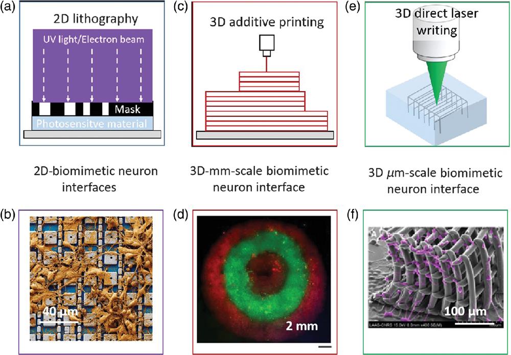
The development of BNIs has witnessed ongoing technological innovations toward achieving more complex biomimetic neuron structures (Fig. 1): from 2D to 3D.45 Different lithographic and bio-printing techniques have been utilized to create microstructures using biologically compatible materials. Primitive designs of biomimetic neuron structures are based on 2D through-holes,35 microtunnels,46 microtroughs,47 and microwells48 on biocompatible materials, such as polydimethylsiloxane parylene and hydrogels. Recent developments of the 3D additive printing technique have also demonstrated its potential in building large-scale 3D BNIs.49 These neuron interfaces have been very effective for studying neuron activities,50,51 and also a platform to realize neuron computing.52 Traditional studies in BNIs generally focus on utilizing the BNIs to assist in the passive study of in-vivo neuronal functions, such as intracellular neuron signals study,17 neuron synaptic study,53 modulation of 2D neuron activities,54 construction of neuronal logic devices,55 and drug release study.56 The key achievements and approaches are summarized in Table 1.
Figure 1.Recent developments of building BNIs at different scales. (a) and (b) Schematic of 2D lithography of BNIs; 2D BNIs fabricated on a CMOS nanoelectrode array improved the nano-bio interface to enable intracellular recording from rat neurons. The device contains a nanoelectrodes, array and records intracellular signals from more than 1700 rat neurons;17 (c) and (d) schematic of 3D additive printing of BNIs; 3D additive printing of bioengineered 3D brain-like layered structures;20 and (e) and (f) schematic of 3D DLW of BNIs; DLW of 3D BNI in hydrogel material.44
However, the current 2D methods cannot achieve the 3D spatial extensions of neuron axons and dendrites, with the largest number of neurons around 1700, still far behind the neuron numbers in animal brains [see Figs. 1(a) and 1(b)].17 In addition, 3D additive printing is able to achieve millimeter-scale neuron interfaces but the fabrication resolution limits its capability of creating 3D BNI with micrometer- or nanometer-scale resolution [see Figs. 1(c) and 1(d)].65–67 One potential solution toward the building of 3D and nanometer-scale BNI lies in the recent development of 3D DLW. A 3D DLW, such as single-beam two-photon DLW and two-beam SPIN, has been widely utilized to produce 3D micro/nanostructures in nanophotonics,68 microfluidics, and biomedical implants.69
3 Principle of 3D DLW
The fundamental phenomenon behind 3D DLW is multi-photon absorption. In this review, we shall concentrate on the theory of two-photon absorption (TPA), which can be extrapolated to three or more photons. In a 3D DLW process [see Fig. 2(a)], the photoinitiator (PI) in the photoresist absorbs two-photon energy from the focused laser beam, generating active species () in the 3D voxel. Hence, when the density of the photo-generated active species is above a threshold, the monomers () in the photoresist become longer polymeric chains, resulting in a phase change (irreversible, e.g., from liquid to solid, or from one phase to another) in the central position of the 3D voxel. While in the focal volume, when the illuminated energy dose is below the threshold (surrounding area of the focal region), the concentration of the generated active species is below the required threshold for complete polymerization. This incomplete polymerization in this area will be removed later during the developing process (bath in solvents, such as isopropanol). Thus, 3D microstructures can be achieved.
Figure 2.Simplified diagram showing the process of 3D DLW and the TPA phenomenon.
The absorption efficiency of photons in the TPA process relies on the square of the illuminated light intensity. This nonlinear absorption of photons results in a smaller feature size narrower than the full width at half-maximum (FWHM) by a magnitude of ,56,70
For every photoresist, the polymerization threshold is a fixed value. Therefore, by decreasing the illuminated intensity of the laser beam slowly until its intensity is higher than the polymerization threshold, the smallest feature size can be obtained, smaller than the diffraction limit compared with single-photon polymerization.
For 3D DLW of microstructures, the line width or feature size and the writing resolution/two-line resolution are the two characteristic parameters, which will determine the dimension and feature size of the microstructures. There are several important factors in a 3D DLW system influencing the line width and the writing resolution:71 (1) the laser source, motion system; (2) equipped optics; and (3) the photoresist or photosensitive material.
3.1 Laser Sources in 3D DLW
For the laser sources used in 3D DLW, pulsed lasers and continuous wave (CW) lasers have both been exploited in 3D DLW.72–74 The final characteristics of the microstructures fabricated by DLW highly rely on the excitation wavelength, the repetition rate of the laser pulse, the operation power of the laser sources, and the optics used in the systems. These performances and the qualities of the equipped optics are also critical for the feature size of the polymerization, such as the focal length and numerical aperture (NA) of the objectives. These properties will influence the energy dose delivered into the photoresist, where the polymerization mechanisms and crosslinking ratio between the polymeric chains influence the subsequent change in the physical phase of the photoresist and the ability of the active polymeric chains to propagate and terminate between each other.75,76
Until recently, femtosecond laser sources are preferred in DLW, such as the Ti:sapphire femtosecond oscillator operating at around 800 nm, and second-harmonic fiber lasers typically operating at 780 nm. A green wavelength (532 nm) amplified ultrafast yttrium aluminium garnet laser has also been used recently because they can provide a higher fabrication resolution with a smaller wavelength and low absorption in a high water content environment.77 It has been proven to be effective in DLW under a high-water-content environment. The pulse lengths () and the repetition rates (50 to 80 MHz) of the laser sources in 3D DLW play significant roles in delivering the energy doses (a few nanojoules per pulse) for the polymerization process, which also relies on the photosensitivity of the material, the PI, and the focusing.
3.2 Fabrication Schemes in 3D DLW
A 3D DLW is a well-established technology for the fabrication of 3D polymer nanostructures and microstructures. In essence, the fabrication schemes of 3D DLW should be considered as an important factor as they will influence the quality of the fabrication, and for different application purposes. To use the 3D focusing voxel to write the 3D structures into the photoresist using the focused laser beam, either the beam focus, or the sample needs to move according to the fabrication scheme that one chooses. The movement of the beam focus can be done with galvanometric scanners (galvo-mirrors), while the movement of the sample can be achieved with high-resolution stages, as is shown in Fig. 3(a).78–81
Figure 3.(a) Schematic of a 3D DLW set-up, including (i) the laser source (ultra-fast pulsed or CW laser); (ii) a motion system consisting of nano-piezo-stages and galvo-mirrors; (iii) beam manipulation optics, which might consist of systems, high-NA objective, etc.; (iv) beam intensity control systems, including a shutter (either an acoustic optical modulator or a mechanical shutter); and (v) a user interface to control the system with a high-performance computer. (b) Layer-by-layer DLW fabrication of a representation of the Oriental Pearl Tower of Shanghai. Right: computer-aided design (CAD) model. Left: SEM image of the fabrication result. (c) Line-by-line fabrication of biomimetic neuron structures.67 Right: CAD model. Left: SEM image of the fabrication result.
Two types of fabrication schemes are demonstrated: “the layer-by-layer fabrication” and “the line-by-line fabrication.” When using the layer-by-layer fabrication scheme, the CAD model of the target 3D microstructures is ‘sliced’ along one direction (usually along the -direction), and each slice is separated with a slicing distance. When the “writing” of each slice is finished, a nanometric translation stage is used to move the sample along the -direction. Using this method, the whole structure can be accomplished. This process is demonstrated in Fig. 3(b), where a 3D miniaturized “Pearl Tower of Shanghai” is fabricated using a layer-by-layer scheme in the laboratory of the Institute of Photonic Chips, the University of Shanghai for Science and Technology.
When using the line-by-line fabrication, there is no need to slice the CAD design, as fabrication can be achieved using the nanoscale stages. Due to the nm-scale accuracy of typical piezoelectric stages, the movement of the writing voxel can be as small as several nanometers, and the fabrication speed can be hundreds of micrometers per second. For structures composed of lines, such as lattice-based photonic crystals and 3D microstructures with high porosity, a line-by-line fabrication scheme is usually used. Figure 3(c) shows a 3D biomimetic neuron being fabricated using this method.67
Other categories of fabrication schemes are classified by whether the used objective is dipped in immersion oil or directly in the photoresists. This difference of these fabrication schemes is to compensate for the distortion resulting from the refractive index difference between the oil and the glass,82 which has been thoroughly discussed in a wide range of literature.
3.3 Materials Used in 3D DLW
From a technical point of view, the photoresist suitable for DLW based on TPA should consist of at least two components: a PI and a monomer. The absorption spectra of these two components should both have a transparent window at the frequency or wavelength () of the operated laser. This transparency window will enable the illuminated light energy to be delivered into the volume of the photoresist without being scattered and absorbed by the bulk of the material. To achieve polymerization based on TPA, the monomer should also have a transparent window around/at the TPA wavelength () of the PI. The success of a proper photoresist also requires the PI to have a high two-photon cross-section,83 which corresponds to a high radical quantum yield and highly active radical species generation ratio. Most of these materials are reviewed along with their applications in the following section.
4 Applications of 3D DLW of Biomimetic Neuron Interfaces
4.1 Biomimetic Neuron Interfaces for Neuron Tissue Engineering
The 3D DLW of BNIs for neuron tissue engineering application has been developed for a decade, with numerous amounts of progress toward the unveiling of the functions of the neurons.69,84–86 For neuron tissue engineering applications, BNIs with 3D microscale features are generally fabricated using 3D DLW. After the fabrication, biological neuron tissues would be embedded and cultured within biomimetic neuron structures. Along with the recent development in scanning electron microscopy (SEM), fluorescence microscopy, and confocal microscopy,87 the functionalities of biological neuron cells can be studied in BNIs. Therefore, 3D DLW of BNIs has demonstrated itself as a useful tool for a wide range of neuroscience research, specifically for the investigation of neural networks in 3D in vitro environments, such as cell force measurement, cell migration, selective cell implants, and microfluidic applications.88 The properties of these 3D structures by DLW, such as mechanical stiffness, geometry, biological, and chemical cues are all factors considered in the design of BNIs.
The utilization of 3D DLW to fabricate 3D microstructures was first introduced with organic materials,89 and proved to be effective in the field of BNIs to study neuron migration,88 as the 3D microenvironment produces higher cell migration speeds than their 2D counterparts. In these studies, organic photopolymers are used for 3D DLW, such as acrylate photopolymers.90 This is because these materials are very easy to be synthesized and have relatively low costs, and most of these materials are transparent at visible or near-infrared wavelengths. Taylia et al. proposed using triacrylate photoresist to fabricate cage-like structures to study the migration and adhesion of the cells in 3D (Fig. 4).58 3D porous structures made of an acrylate photopolymer were fabricated inside the closed microchannel of a commercially available polymer chip for analysis of directed cell invasion.84
Figure 4.The 3D BNIs for a 3D real-time neuron migration study.58 (a) Bright-field optical microscopic image showing the distribution of cells in a pore-sized microstructure 5 h after seeding the cells. (b) The 3D FM image showing the 3D distribution of the cells inside a scaffold 24 h after seeding the cells. (c) Top view of the fluorescent microscope of the cells in pore-sized scaffolds showing the non-uniform distribution of the cells under varied physical obstructions. (d) Tracking of a typical cell migration phenomenon in a scaffold.
SU-8 is a negative, epoxy-based photoresist commonly used for the fabrication of microstructures with high aspect ratios for its excellent mechanical properties, and it has been widely used in 3D DLW. SU-8 has shown its advantages in thermal stability, chemical inertness, high aspect ratio, and high crosslinking propensity, and it has been widely used to construct biomedical sensors, where the solvent-induced swelling could be minimized.59,91 SU-8 based microelectrodes have been fabricated to track the nerve action potential signals within the peripheral nervous system in the rat central nervous system.92
Hybrid photosensitive materials have been developed for DLW due to their commercial availability and their superb properties such as high Young’s modulus, optical transparency, and thermal/chemical stability,93 especially because they can be fabricated with the laser at low temperatures. Three-dimensional tubular microtowers were designed and fabricated in ORMOCOMP® (a commercially available photoresist) to function as neuronal cell culture platforms (see Fig. 5).60 Due to the 3D nature of the structures, it is proved that efficient long-term 3D culturing of human neuronal cells can be achieved (the neuron cells are derived from stem cells), and these 3D structures can support the neural orientation and the neural network formation in 3D. In addition, these microtowers are designed with or without intra-luminal guidance cues and/or openings in the tower, demonstrating the strong mechanical properties of hybrid photoresists. Another most widely used photoresist is ORMOCER®, and its variants (ORMOCOMP® and ORMOCLEAR®). This type of photoresist is commercially available94 and has been used to fabricate microstructures to study the mobilization of the bio-tissues.59
Figure 5.3D BNIs for supporting the neurite/neuron orientation and 3D network formation. (a) Left: SEM images and the CAD model of the microtowers fabricated by 3D DLW. SEM images of neuronal cells on the microtower after one week of cell culture.60 Right: 3D reconstruction of the confocal microscopic image showing the neuronal cell distribution on the tower. The neuronal markers are MAP-2 (green), β-tubulin III (red), and DAPI (blue). (b) Left: SEM images of neuron-cages fabricated by DLW using ORMOCER®.59 Right: confocal microscope images of type II and type III neurocages after eight days of culturing. MAP-2 (green) and astrocytes GFAP (red) are used to stain the neuronal cells.
Other types of hybrid photoresists that have been widely used in 3D DLW are “zirconium hybrid organic-inorganic/The FORTH” photoresist,82,95 and SZ2080;96,97 both of these photoresists are optically transparent and mechanically strong.98 These properties lead to low shrinkage, and thus make these hybrid photoresists suitable for applications sensitive to structural deformations (such as nanophotonics applications), since additional design steps are not needed to compensate for distortions. Its properties lead to a wide range of applications in nanophotonics and bio-tissue engineering.99 Niches made of SZ2080 were proved to be effective to home, colonizing, and proliferating mesenchymal stem cells due to the favorable conditions provided in the microstructure.97 3D network-like structures were fabricated as scaffolds using ORMOCOMP for cardiomyocyte contraction force measurements (see Fig. 6).61 Cell force at the nanonewton scale can be measured by calibrating the shape deformation of the beams in the network.
Figure 6.Hybrid photoresist fabricated by 3D DLW of a 3D network-like structure for neuron force measurement, the photoresist is Ormocomp®.61 (a) and (b) The 3D reconstruction of a confocal microscopic image of cardiomyocyte cells attached in the network-like microstructure, where the posts are connected by beams with a diameter of (oblique view and top view). (c) The SEM image of a fully 3D network-like microstructure for cell force measurement. The sample is labeled by F-actin (green) and A-actinin (red). (d) Video frames of the deformation process of the beam in contact with the cell, where the bending of the beam can represent the cell force during one cycle of contraction (time in seconds). (e) The experimental plot of force–beam deflection, where the cell force can be calibrated by the deformation of the beams.
Chemically modified natural polymers, such as polylactide-based (PLA) materials, have been fabricated by DLW multi-photon polymerization for neural tissue engineering scaffolds. Typically, submicrometer structures can be produced in PLA and hyaluronic acid (HA) photoresist by DLW using a femtosecond Ti:sapphire laser to promote the neuron growth guidance [see Figs. 7(a) and 7(b)].50,62 Photopolymerized thin-film PLA substrates and 3D microstructures were fabricated, and cell culture results showed that the photocured PLA maintained a relatively high Schwann cell purity (99%). The microenvironment also enabled cell proliferation over the length of seven days. In addition, the substrate supports Schwann cells to adhere to different directions where bi-polar and tri-polar morphologies were observed [see Fig. 7(c)].63 The PLA material is suitable for applications in fabricating neural scaffolds in nerve repair.100
Figure 7.Modified and natural polymers fabricated by 3D DLW for 3D neuron network guidance. (a) Microstructures fabricated using PLA to support PC12 neuronal cell growth. After five days of culturing, PC12 cells proliferate in woodpile structures (, , and magnifications are shown).50 (b) Microstructures fabricated on an HA hydrogel surface to promote the guidance growth of hippocampal progenitors (E16).62 Fluorescence image of the neuronal marker b-III tubulin (green) after fixation. Scale bar, . (c) A live C. elegans worm encapsulated in a BSA structure on a photopolymerized microstructure (base).63
Biodegradable hydrogel (HA) materials,101–104 have also attracted huge amounts of attention during recent years in biomedical research, such as functional biosensors, bio-compatible wearable devices, and self-healing materials.105–107 Due to their water absorbent property, high flexibility in shape deformation, and non-toxicity, especially in the recent development of fabricating hydrogel microstructures using 3D DLW, polyethylene glycol (PEG)108 is a cost-effective and Food and Drug Administration (FDA) approved synthetic hydrogel. PEG is also very compatible with a lot of different formulations for 2D and 3D additive printing. It was recently found that the crosslinking by 3D DLW of PEG‐based materials, which can be cleaved and erased in water (without the need for acidic or basic additives), hold the potential for the facile modification and backbone degradation of polyether‐containing materials in general. Polyethylene glycol diacrylate (PEGda) is a variant of PEG, and it can be synthesized or is commercially available.109 Both PEG and PEGda have been widely used in fabricating 3D microstructures in neuron tissue engineering for their high biocomparability and versatility in adapting to various types of PIs.110 The crosslinked protein inside a hydrogel has been studied as scaffolds for neural cell guidance, and it was proven that complex 3D architectures can enhance the cell culture efficiency and guidance through both chemical and topographical cues, providing an effective pathway toward cell relocation and migration at micrometer scales for in vivo environments [see Fig. 7(b)].62
Other hydrogel materials such as fibrogen and fibronectin, collagen, and bovine serum albumin (BSA) have been utilized in DLW for neuron tissue engineering. These materials are either natural polymers or proteins.111–113 As natural polymers and proteins, they have proven their biocompatibility in neuron tissue engineering. A live Caenorhabditis elegans worm was encapsulated in polymerized BSA as an in-vivo platform to study the nerve function in real-time [see Fig. 7(c)].63 It is proved in this work that neuron signal transmission can be detected through microelectrodes based on BSA microstructures. The mixture of BSA and modified gelatin was also studied to create well-defined DLW scaffolds.114
4.2 Biomimetic Neuron Interfaces for Artificial Neural Networks
Recent development in 3D DLW of BNIs has also witnessed several advances in ANNs, as DLW enables the 3D fabrication capability at the micro/nanoscale. This fits perfectly into the desire for a parallel and energy-efficient interconnect in neuron-inspired computing.115 By resembling the natural counterpart (BNNs), fully or densely connected layers are the desired principal topology in ANNs, which enables massively parallel processing. A fractal topology for fully connected layers was designed and fabricated [shown in Fig. 8(a)] using 3D DLW.64 These well-designed 3D connected waveguides functioned as convoluting optical interconnects in convolutional neural networks (CNNs). However, the low connection density ( artificial neuron connection array) and the high crosstalk between the waveguides remain a challenging task in this field, with several potential progresses in DLW to reduce the loss in 3D waveguides fabricated by DLW.117
Figure 8.BNIs for ANNs. (a) The 3D optical interconnects fabricated by 3D DLW.64 The interconnected structure functions as a Haar filter, which is regarded as a fundamental unit in CNNs. (b) Neuron-inspired Steiner tree low-density metastructures; the scale bar is .116
BNIs also have been demonstrated to be a family of low-density metastructures fabricated by 3D DLW [see Fig. 8(b)].116 This type of metastructure resembles the shortest connection distance in BNNs, and functions as a unique low-density metamaterial hosting triple degeneracy Dirac-like points. It is also envisioned that Steiner tree metastructures might be a platform to realize zero-index material and photonic neural networks for their high degree of connectivity. Neuron-inspired nanopores that resemble the ion channels in neuron membranes have been fabricated,118 which might facilitate the application of artificial membranes in biological applications.
5 ANNs Enabled Efficient DLW for Large-Scale Biomimetic Neuron Interfaces
As discussed above, the DLW of BNIs has been developed for almost a decade, with various geometrical designs and materials developed and utilized for neural tissue engineering and functional ANNs applications. The future development of BNIs requires an efficient DLW system to achieve large-scale fabrication, where a large amount of data in the DLW needs to be processed efficiently.119,120 To satisfy this aim, developing an ANNs-enabled DLW system is the most interesting and challenging field. This section examines emerging ANNs technologies that will play an important role in the future progress in DLW of large BNIs.
ANNs have attracted considerable attention as an advanced method to solve complex practical problems in different areas.121 A simplified but typical data flow of a feed-forward ANN is shown in Fig. 9(a). In this ANN, the input data move in a forward direction. A series of data nodes (artificial neurons) are integrated to form the layer of input. Within the ANNs, the input signal is passed through one or more hidden layers. At the end of this network, the output layer generates the predicted results. Different from the current von Neumann computer that performs tasks by the pre-design of the program, the ANNs can learn to run a task through a group of training datasets. For example, one of the typical learning processes is the supervised learning method by updating weights with the backpropagation errors between known target values and the output values.122 Choosing appropriate hyper parameters in a neural network has a vital role in the training of ANNs models. The final step is to evaluate the performance of the model by calculating the error in the prediction of outputs. The smaller difference between errors in training data and testing data indicates the more superior generalization of the model.
Figure 9.(a) The structure of feed-forward ANNs. (b) The effective parameters in the 3D DLW process.
Developing an accurate ANNs algorithm for DLW to describe the relationship between output and input variables in the DLW process is of great importance to tackling challenges induced by the dynamic nature of DLW.123,124 As is discussed in Sec. 3, the most influential parameters associated with DLW can be generalized into geometrical parameters (fabrication scheme), material parameters (choice of the photoresists), and system parameters (laser setup, etc.). Based on the results from theoretical and experimental data, the performance of DLW can be enhanced significantly by choosing these parameters adequately. The effective parameters in DLW are shown in Fig. 9(b).
For instance, to improve the laser focusing efficiency and quality, ANNs enabled adaptive optics technology was used for fast focusing of a Gaussian beam with wave-front aberration correction and recovery of near-diffraction-limited focal spots. The ANN was trained to determine low-order aberrations from distorted point spread function images detected using a complementary metal-oxide semiconductor (CMOS) camera with Zernike mode coefficients [shown in Fig. 10(a)].125,127 Similarly, various ANNs have been applied to laser processing techniques to optimize the parameters. Taguchi and his group created a novel ANNs-based technique to effectively optimize the laser welding parameter,126,128 and the combination of these two methods can also obtain good, optimized fabrication results [shown in Fig. 10(b)]. Taguchi’s method is widely used in optimizing the laser processing parameters; this approach can reduce the time and cost for the experimental investigations.129 To improve the depth-width ratio of the laser welding, Ai et al.130 applied the Taguchi method to optimize three welding parameters, i.e., the laser power, welding speed, and focal position. Results showed the reliability and effectiveness of the proposed method. In addition, ANNs for path optimization can improve the fabrication efficiency (in terms of time and cost), while the traditional fabrication schemes of DLW are based on line-by-line scanning techniques and will cost an unachievable amount of time.131
Figure 10.ANNs-based adaptive optics technology for laser focusing optimization. (a) ANNs-based adaptive optics techniques enable the aberration correction of Gaussian-shaped laser beams.125 (b) Experimental results of Kerf acquired without and with optimized focusing parameters.126
5.2 ANNs-Enabled Inverse Design of Biomimetic Neuron Interfaces
Recent research in ANNs has been able to help scientists reveal the brain’s structure,132 where the 3D wiring diagram of neurons in the animal brain can be automatically distinguished by CNNs. These structural data of BNNs can be inversely translated into novel neuron models to create BNIs based on the principles from biomimicry.
On the other hand, ANNs can also contribute to the design of complex biomimetic interfaces and biomimetic geometry design133 where the geometry of biomimetic interfaces can be mathematically calculated with an interactive ANNs algorithmic description. Such methods have been widely used in computer chip design to solve the high dimensional connection and energy efficiency (power distribution/heat dissipation) problems.134 Functional BNIs based on nanophotonics can be inverse designed and incorporated using ANNs. Such inverse design methods based on ANNs can improve the performance of a waveguide-based multiplexer and de-coupler.41
To date, even though few studies have been done on the direct integration of ANNs and DLW, the possible concept of ANNs implementation in 3D large-scale additive printing has been demonstrated to fix the fabrication failure without interruption of the 3D printing processing and become a revolutionary field in health care.135 Therefore, the integration of DLW and ANNs for BNIs would have great potential in the next generation of neural tissue engineering and functional ANNs applications.
6 Conclusion and Outlook
This article reviews the fast developing field of 3D direct laser writing of biomimetric neuron interfaces. It is demonstrated that 3D DLW represents a powerful technique to fabricate 3D BNIs for neuron tissue engineering and ANNs. Indeed, 3D BNIs have proven to be a better ensemble of BNNs compared with the currently popular 2D systems.136 Although this field is witnessing a transition from simple to architecturally complex structures, large-scale BNIs could not be facilely achieved using current 3D DLW due to the low fabrication speed and poor quality control.
To fully achieve the scale-up and efficient fabrication of BNIs, the integration of ANNs algorithms with DLW is highly necessary so that the computational cost, qualification cost, and data acquisition/processing cost can be dramatically reduced.137,138 In addition, the further optimization of photoresist materials in DLW is also necessary. This includes but is not limited to the development of water-soluble PIs with high TPA cross sections,139 development of new composite materials, such as conductive photopolymers and photonic photoresists,140,141 so that the fabricated 3D BNIs can be applied with two-photon holography optogenetics,142,143 where the functionality of the neurons can be excited and visualized in real time. Along with the ongoing research progress in DLW-enabled quantum dots,144 artificial memristors,145 and biomimetic synapses,146 DLW could also enable the realization of BNIs for innovative ANNs.
Haoyi Yu received his MSc degree from Nankai University in 2015 and his PhD from RMIT University in Australia in 2019. Currently, he is appointed as a research fellow at the Centre for Artificial-Intelligence Nanophotonics (CAIN), and Institute of Photonic Chips, University of Shanghai for Science and Technology. His research interests include nanophotonics, artificial neural networks, and biophotonics. He has published more than 10 research works in such journals as Advanced Science, Light: Science and Applications, and Optics Express.
Qiming Zhang received his PhD in optical science from Fudan University in 2011. He had been a senior researcher of RMIT in Australia before he joined USST in 2019. He has published more than 30 papers in such journals as Science, Nature Photonics, Nature Communications, Nature Review Materials, and Optics Letters. His research interests include center on artificial intelligence nanophotonics device, optical information storage, and femtosecond optical processing.
Xi Chen received his PhD from Queensland University of Technology in 2010, and joined University of Shanghai for Science and Technology in 2019. His research fields are artificial intelligence materials, laser fabrication, and supercapacitors. He has published SCI papers in international journals such as Advanced Materials and Nano Letters.
Haitao Luan received his MSc degree from University of Kassel in 2013 and commenced to Centre for Micro-Photonics (CMP) to pursue a PhD studentship. He received his PhD from RMIT University in 2019 and subsequently was appointed a research fellow at Centre for Artificial-Intelligence Nanophotonics (CAIN) in University of Shanghai for Science and Technology. Currently, he is a research professor and an assistant director (Innovation) of Institute of Photonic Chips (IPC) of USST.
Min Gu is an executive chancellor of the University Council and a distinguished professor of University of Shanghai for Science and Technology. He was a distinguished professor and an associate deputy vice-chancellor at RMIT University and a laureate fellow of the Australian Research Council. He is an elected fellow of the Australian Academy of Science and the Australian Academy of Technological Sciences and Engineering, and foreign fellow of the Chinese Academy of Engineering. He was awarded the Einstein Professorship, the W. H. (Beattie) Steel Medal, the Ian Wark Medal, the Boas Medal, the Victoria Prize for Science and Innovation, the Dennis Gabor Award, and the Emmett N. Leith Medal.
[135] A. Banerjee et al. Artificial intelligence in 3D printing: a revolution in health care. Emerging Applications of 3D Printing During CoVID 19 Pandemic, 57-79(2022).
Haoyi Yu, Qiming Zhang, Xi Chen, Haitao Luan, Min Gu, "Three-dimensional direct laser writing of biomimetic neuron interfaces in the era of artificial intelligence: principles, materials, and applications," Adv. Photon. 4, 034002 (2022)