• Advanced Photonics
  • Vol. 2, Issue 6, 064001 (2020)
Yifeng Xiong and Fei Xu*
Author Affiliations
  • Nanjing University, College of Engineering and Applied Sciences, Nanjing, China
  • show less
    DOI: 10.1117/1.AP.2.6.064001 Cite this Article Set citation alerts
    Yifeng Xiong, Fei Xu. Multifunctional integration on optical fiber tips: challenges and opportunities[J]. Advanced Photonics, 2020, 2(6): 064001 Copy Citation Text show less
    Multifunctional integration on optical fiber tips. Traditional optical, electrical, acoustic, thermal, biological, and chemical structures have been miniaturized and integrated onto optical fiber tips.
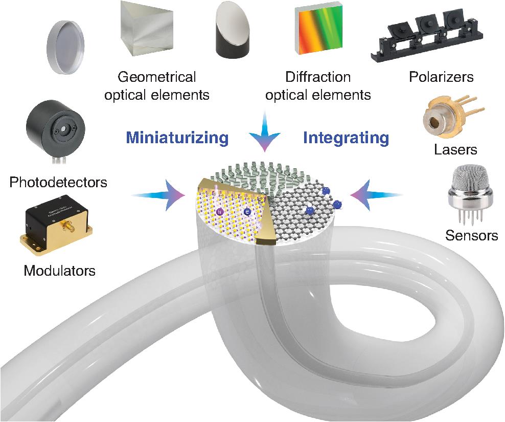
    Fig. 1. Multifunctional integration on optical fiber tips. Traditional optical, electrical, acoustic, thermal, biological, and chemical structures have been miniaturized and integrated onto optical fiber tips.
    Tree diagram of the fabrication technologies for LOF-tip. The “top down” and “bottom up” methodologies involve fabricating the nanomaterials or nanostructure on the fiber tips directly, while the material transfer methodologies involve fabricating the nanomaterials or nanostructure separately on a planar substrate before transferring the prepared structure onto the fiber tips.
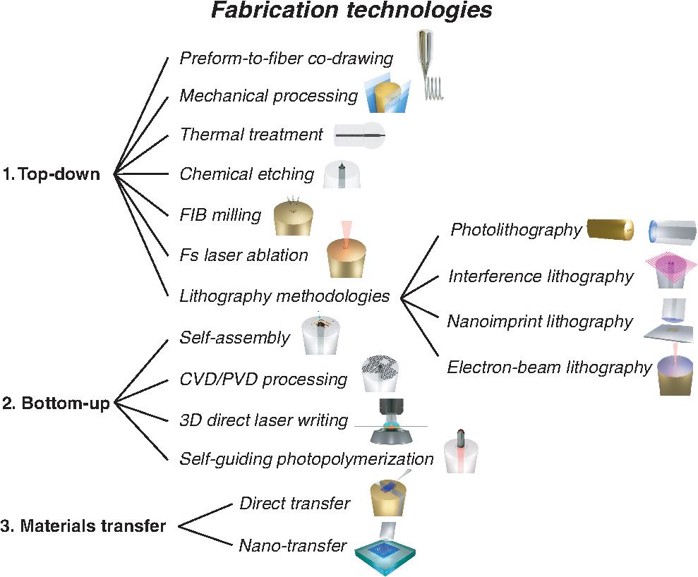
    Fig. 2. Tree diagram of the fabrication technologies for LOF-tip. The “top down” and “bottom up” methodologies involve fabricating the nanomaterials or nanostructure on the fiber tips directly, while the material transfer methodologies involve fabricating the nanomaterials or nanostructure separately on a planar substrate before transferring the prepared structure onto the fiber tips.
    Schematic of the mechanical fabrication processes for electrodes on an optical fiber tip.38" target="_self" style="display: inline;">38 First, lapping films are used to remove a portion of the precoated gold from the fiber sidewall. Then, an electrode on a fiber facet is fabricated by scratching the gold layer using a tapered tungsten needle.
    Fig. 3. Schematic of the mechanical fabrication processes for electrodes on an optical fiber tip.38 First, lapping films are used to remove a portion of the precoated gold from the fiber sidewall. Then, an electrode on a fiber facet is fabricated by scratching the gold layer using a tapered tungsten needle.
    Methods to obtain a thin photoresist film on optical fiber endfaces. (a) Schematic illustration of the “dip and vibration” method.85" target="_self" style="display: inline;">85–87" target="_self" style="display: inline;">–87 (b) Schematic illustration of the spin-coating method. The optical fiber is fixed to a perforated rotating chunk.88" target="_self" style="display: inline;">88
    Fig. 4. Methods to obtain a thin photoresist film on optical fiber endfaces. (a) Schematic illustration of the “dip and vibration” method.8587" target="_self" style="display: inline;">87 (b) Schematic illustration of the spin-coating method. The optical fiber is fixed to a perforated rotating chunk.88
    Schematic illustration of the NI process of optical fibers. (a) NI process based on thermal softening. The optical fiber is aligned and placed in contact with the heated mold to transfer patterns onto the fiber tip. (b) NI process based on lithography. The optical fiber is precoated with polymer, then aligned, and placed in contact with the mold, with patterns transferred to the polymer layer via the exposure procedure.
    Fig. 5. Schematic illustration of the NI process of optical fibers. (a) NI process based on thermal softening. The optical fiber is aligned and placed in contact with the heated mold to transfer patterns onto the fiber tip. (b) NI process based on lithography. The optical fiber is precoated with polymer, then aligned, and placed in contact with the mold, with patterns transferred to the polymer layer via the exposure procedure.
    Schematic illustration of the EBL process to make metallic patterns on optical fibers. (a) A layer of electron beam resist is first coated on the cleaved optical fiber, followed by depositing a thin metal film to improve the conductivity of the fiber. (b) A layer of metal is first deposited on the optical fiber, followed by a coating layer of electron beam resist.
    Fig. 6. Schematic illustration of the EBL process to make metallic patterns on optical fibers. (a) A layer of electron beam resist is first coated on the cleaved optical fiber, followed by depositing a thin metal film to improve the conductivity of the fiber. (b) A layer of metal is first deposited on the optical fiber, followed by a coating layer of electron beam resist.
    3D direct laser writing technique based on TPL/MPL. (a) Schematic illustration of the TPL/MPL fabrication system, including an optical fiber fixed in fiber holders, a photoresist, a glass slide, optical matching oil, and an objective lens. (b1)–(b3) False-color SEM images of a compound microlens system on a fiber endface. (b4)–(b6) False-color SEM images of a woodpile face-centered tetragonal PC created on a fiber endface.131" target="_self" style="display: inline;">131 Copyright 2011, Optical Society of America. (c1)–(c3) Different functional optical elements integrated on fiber tips. The scale bars are 25 μm.132" target="_self" style="display: inline;">132 Copyright 2016, Springer Nature. (d1), (d2) False-color SEM image and the rendered view of a polarizing beam splitter on a fiber endface. The scale bars are 10 μm.133" target="_self" style="display: inline;">133 Copyright 2018, Optical Society of America.
    Fig. 7. 3D direct laser writing technique based on TPL/MPL. (a) Schematic illustration of the TPL/MPL fabrication system, including an optical fiber fixed in fiber holders, a photoresist, a glass slide, optical matching oil, and an objective lens. (b1)–(b3) False-color SEM images of a compound microlens system on a fiber endface. (b4)–(b6) False-color SEM images of a woodpile face-centered tetragonal PC created on a fiber endface.131 Copyright 2011, Optical Society of America. (c1)–(c3) Different functional optical elements integrated on fiber tips. The scale bars are 25  μm.132 Copyright 2016, Springer Nature. (d1), (d2) False-color SEM image and the rendered view of a polarizing beam splitter on a fiber endface. The scale bars are 10  μm.133 Copyright 2018, Optical Society of America.
    Schematic illustration of the micromanipulation method to transfer 2D materials onto the optical fiber electrodes to fabricate photodetectors, taking graphene as an example.36" target="_self" style="display: inline;">36 First, a PMMA film is spin-coated on the graphene. After removing the original substrate, the PMMA-graphene composite film is transferred to a glass slide via the wet-transfer method. A tapered optical fiber is used to scratch and separate a certain shape of the PMMA-graphene film and transfer it onto the electrodes on the optical fiber endface. Then, the fiber is heated to improve the contact between the composite film and the fiber endface. Finally, the PMMA is removed, and the graphene layer is bonded strongly to the fiber glass and the metal electrodes.
    Fig. 8. Schematic illustration of the micromanipulation method to transfer 2D materials onto the optical fiber electrodes to fabricate photodetectors, taking graphene as an example.36 First, a PMMA film is spin-coated on the graphene. After removing the original substrate, the PMMA-graphene composite film is transferred to a glass slide via the wet-transfer method. A tapered optical fiber is used to scratch and separate a certain shape of the PMMA-graphene film and transfer it onto the electrodes on the optical fiber endface. Then, the fiber is heated to improve the contact between the composite film and the fiber endface. Finally, the PMMA is removed, and the graphene layer is bonded strongly to the fiber glass and the metal electrodes.
    The paradigm of multifunctional structures integrated on optical fiber tips. The fiber tip devices were classified with respect to functional structure configuration, including (top left) the 3D miniature micro-optics structures, (top right) 2D textured nano-optics surfaces, and (bottom) electrodes integrated on fiber tips.
    Fig. 9. The paradigm of multifunctional structures integrated on optical fiber tips. The fiber tip devices were classified with respect to functional structure configuration, including (top left) the 3D miniature micro-optics structures, (top right) 2D textured nano-optics surfaces, and (bottom) electrodes integrated on fiber tips.
    Micro-optical elements integrated on optical fiber tips. (a) Phase masks on fiber endfaces for spatial beam intensity shaping. (a1), (a2) SEM images of a diffractive optical element on an optical fiber endface. (a3), (a4) Measured intensity distributions for (a3) the doughnut-shaped and (a4) top-hat-shaped diffractive optical elements.140" target="_self" style="display: inline;">140 Copyright 2016, Optical Society of America. (b) High RI Fresnel lens on a fiber endface for efficient light focusing. (b1), (b2) SEM images of the Fresnel lens on a fiber. (b3), (b4) Light intensity distributions of (b3) a bare single-mode fiber and (b4) a fiber with Fresnel lens. (b5) The corresponding intensity profiles of the light intensity distributions.194" target="_self" style="display: inline;">194 Copyright 2016, Optical Society of America. (c) Suspended polymer microrings on a multicore fiber endface for multiple gas sensing. (c1) SEM image of the optical tentacle on the fiber endface. (c2) Cycle tests for the sensing reversibility of the optical tentacle in three types of vapor.147" target="_self" style="display: inline;">147 Copyright 2020, Optical Society of America.
    Fig. 10. Micro-optical elements integrated on optical fiber tips. (a) Phase masks on fiber endfaces for spatial beam intensity shaping. (a1), (a2) SEM images of a diffractive optical element on an optical fiber endface. (a3), (a4) Measured intensity distributions for (a3) the doughnut-shaped and (a4) top-hat-shaped diffractive optical elements.140 Copyright 2016, Optical Society of America. (b) High RI Fresnel lens on a fiber endface for efficient light focusing. (b1), (b2) SEM images of the Fresnel lens on a fiber. (b3), (b4) Light intensity distributions of (b3) a bare single-mode fiber and (b4) a fiber with Fresnel lens. (b5) The corresponding intensity profiles of the light intensity distributions.194 Copyright 2016, Optical Society of America. (c) Suspended polymer microrings on a multicore fiber endface for multiple gas sensing. (c1) SEM image of the optical tentacle on the fiber endface. (c2) Cycle tests for the sensing reversibility of the optical tentacle in three types of vapor.147 Copyright 2020, Optical Society of America.
    Optical fiber-based SERS probes. (a) Schematic depiction of the measurement setup for characterizing an SERS probe. Inset: SEM image of an array of Au optical antennas on a fiber endface.166" target="_self" style="display: inline;">166 Copyright 2009, American Chemical Society. (b) SEM image of the Ag-coated nanopillar array on a fiber endface used for SERS.96" target="_self" style="display: inline;">96 Copyright 2012, Optical Society of America. (c) SEM image of nanoscale honeycomb structures on a fiber endface for SERS.66" target="_self" style="display: inline;">66 Copyright 2005, Optical Society of America. (d) SERS-on-a-tip probes based on a nanoarray on an optical fiber endface.145" target="_self" style="display: inline;">145 (d1) Schematic illustration of the mechanism for Raman scattering enhancement. (d2), (d3) SEM image of the cross-spike array on an optical fiber tip. Copyright 2020, WILEY-VCH Verlag GmbH & Co. KGaA, Weinheim.
    Fig. 11. Optical fiber-based SERS probes. (a) Schematic depiction of the measurement setup for characterizing an SERS probe. Inset: SEM image of an array of Au optical antennas on a fiber endface.166 Copyright 2009, American Chemical Society. (b) SEM image of the Ag-coated nanopillar array on a fiber endface used for SERS.96 Copyright 2012, Optical Society of America. (c) SEM image of nanoscale honeycomb structures on a fiber endface for SERS.66 Copyright 2005, Optical Society of America. (d) SERS-on-a-tip probes based on a nanoarray on an optical fiber endface.145 (d1) Schematic illustration of the mechanism for Raman scattering enhancement. (d2), (d3) SEM image of the cross-spike array on an optical fiber tip. Copyright 2020, WILEY-VCH Verlag GmbH & Co. KGaA, Weinheim.
    Metasurfaces on optical fiber tips. (a) An optical fiber MT for beam steering and coupling. (a1) Schematic view of the MT with a plasmonic MS fabricated on the endface. (a2) Illustration of the MT operating principle. (a3) Geometry of the rectangular nanoaperture realized in an Au layer.78" target="_self" style="display: inline;">78 Copyright 2016, Springer Nature. (b) Schematic illustration of an MS-covered optical fiber tip for all-optical signal modulation based on coherent absorption. The insets are SEM images of the device, black scale bar: 100 μm, gray scale bar: 1 μm. Copyright 2018, Springer Nature.
    Fig. 12. Metasurfaces on optical fiber tips. (a) An optical fiber MT for beam steering and coupling. (a1) Schematic view of the MT with a plasmonic MS fabricated on the endface. (a2) Illustration of the MT operating principle. (a3) Geometry of the rectangular nanoaperture realized in an Au layer.78 Copyright 2016, Springer Nature. (b) Schematic illustration of an MS-covered optical fiber tip for all-optical signal modulation based on coherent absorption. The insets are SEM images of the device, black scale bar: 100  μm, gray scale bar: 1  μm. Copyright 2018, Springer Nature.
    Optical tweezers based on a double nanohole on the fiber endface.272" target="_self" style="display: inline;">272 (a) SEM image of the active region of the fiber. (b) SEM image of the finished double nanohole milled in the active region of the fiber. (c) Schematic illustration of the characterization setup of the optical tweezers. (d), (e) Trapping events for individual 40- and 20-nm diameter PS spheres, respectively, which are detected via the change in transmission. Copyright 2014, Optical Society of America.
    Fig. 13. Optical tweezers based on a double nanohole on the fiber endface.272 (a) SEM image of the active region of the fiber. (b) SEM image of the finished double nanohole milled in the active region of the fiber. (c) Schematic illustration of the characterization setup of the optical tweezers. (d), (e) Trapping events for individual 40- and 20-nm diameter PS spheres, respectively, which are detected via the change in transmission. Copyright 2014, Optical Society of America.
    NEMS on fiber tips. (a) Schematic of the optical fiber magnetometer based on a graphene NEMS. (b) Microscope image of the endface of the fiber sensor.
    Fig. 14. NEMS on fiber tips. (a) Schematic of the optical fiber magnetometer based on a graphene NEMS. (b) Microscope image of the endface of the fiber sensor.
    All-in-FPD. (a) FPD integrated with a film of MoS2.38" target="_self" style="display: inline;">38 (a1) Schematic of the FPD with a MoS2 film deposited above the electrodes. Inset: The cross-sectional part of the FPD and the measurement setup. (a2) The optical microscope image of the FPD. The scale bar is 20 μm. (a3) The SEM image of the FPD. The scale bar is 50 μm. Reproduced with permission from the Royal Society of Chemistry. (b) High-sensitivity FPD with an integrated CsPbBr3-graphene hybrid structure.164" target="_self" style="display: inline;">164 (b1), (b2) Schematic of the materials structures and device configuration of the FPD. (b3), (b4) Photograph and microscope image of an FPD. The scale bar is 20 μm. Copyright 2017, Optical Society of America. (c) Broadband FPD based on a graphene-MoS2-WS2 heterostructure.36" target="_self" style="display: inline;">36 (c1), (c2) Schematic representation of the FPD. (c3) SEM image of the FPD. The scale bar is 20 μm. Copyright 2018, WILEY-VCH Verlag GmbH & Co. KGaA, Weinheim. (d) Schematic view of the COF-graphene-based FPD, which can be used as a gas sensor. Inset: The gas molecule absorption and charge transfer at the surface of the COF-graphene film.37" target="_self" style="display: inline;">37 Copyright 2020, WILEY-VCH Verlag GmbH & Co. KGaA, Weinheim.
    Fig. 15. All-in-FPD. (a) FPD integrated with a film of MoS2.38 (a1) Schematic of the FPD with a MoS2 film deposited above the electrodes. Inset: The cross-sectional part of the FPD and the measurement setup. (a2) The optical microscope image of the FPD. The scale bar is 20  μm. (a3) The SEM image of the FPD. The scale bar is 50  μm. Reproduced with permission from the Royal Society of Chemistry. (b) High-sensitivity FPD with an integrated CsPbBr3-graphene hybrid structure.164 (b1), (b2) Schematic of the materials structures and device configuration of the FPD. (b3), (b4) Photograph and microscope image of an FPD. The scale bar is 20  μm. Copyright 2017, Optical Society of America. (c) Broadband FPD based on a graphene-MoS2-WS2 heterostructure.36 (c1), (c2) Schematic representation of the FPD. (c3) SEM image of the FPD. The scale bar is 20  μm. Copyright 2018, WILEY-VCH Verlag GmbH & Co. KGaA, Weinheim. (d) Schematic view of the COF-graphene-based FPD, which can be used as a gas sensor. Inset: The gas molecule absorption and charge transfer at the surface of the COF-graphene film.37 Copyright 2020, WILEY-VCH Verlag GmbH & Co. KGaA, Weinheim.
    Yifeng Xiong, Fei Xu. Multifunctional integration on optical fiber tips: challenges and opportunities[J]. Advanced Photonics, 2020, 2(6): 064001
    Download Citation