1School of Civil Engineering, Hefei University of Technology, Hefei 230009, China
2Jiangsu Key Laboratory of Engineering Mechanics, Southeast University, Nanjing 210096, China
3Key Laboratory of MicroNano Powder and Advanced Energy Materials of Anhui Higher Education Institute, School of Chemistry and Materials Engineering, Chizhou University, Chizhou 247000, China
Li Zhong, Xiaobao Li, Wei Wang, Xinle Xiao. Electromechanical and photoelectric properties of a novel semiconducting Janus InGaSSe monolayer[J]. Journal of Semiconductors, 2023, 44(1): 012701
Copy Citation Text
In recent years, Janus two-dimensional (2D) materials have received extensive research interests because of their outstanding electronic, mechanical, electromechanical, and optoelectronic properties. In this work, we explore the structural, electromechanical, and optoelectronic properties of a novel hypothesized Janus InGaSSe monolayer by means of first-principles calculations. It is confirmed that the Janus InGaSSe monolayer indeed show extraordinary charge transport properties with intrinsic electron mobility of 48 139 cm2/(V·s) and hole mobility of 16 311 cm2/(V·s). Both uniaxial and biaxial strains can effectively tune its electronic property. Moreover, the Janus InGaSSe monolayer possesses excellent piezoelectric property along both in-plane and out-of-plane directions. The results of this work imply that the Janus InGaSSe monolayer is in fact an efficient photocatalyst candidate, and may provide useful guidelines for the discovery of other new 2D photocatalytic and piezoelectric materials.In recent years, Janus two-dimensional (2D) materials have received extensive research interests because of their outstanding electronic, mechanical, electromechanical, and optoelectronic properties. In this work, we explore the structural, electromechanical, and optoelectronic properties of a novel hypothesized Janus InGaSSe monolayer by means of first-principles calculations. It is confirmed that the Janus InGaSSe monolayer indeed show extraordinary charge transport properties with intrinsic electron mobility of 48 139 cm2/(V·s) and hole mobility of 16 311 cm2/(V·s). Both uniaxial and biaxial strains can effectively tune its electronic property. Moreover, the Janus InGaSSe monolayer possesses excellent piezoelectric property along both in-plane and out-of-plane directions. The results of this work imply that the Janus InGaSSe monolayer is in fact an efficient photocatalyst candidate, and may provide useful guidelines for the discovery of other new 2D photocatalytic and piezoelectric materials.
Introduction
Renewable and clean energy sources are highly desired and receive considerable attentions because of increasing energy demands and environmental pollution issues. As one of the most important clean-energy harvesting strategies, photocatalytic water-splitting by utilizing inexhaustible solar energy is expected to be a promising way to address those worldwide energy issues. It is well known that the performance of photocatalysts is a key assessment criterion of the photocatalytic reaction process. In general, an ideal photocatalytic material should possess an appropriate band gap (e.g., ~2 eV) with suitable band edge positions, a high charge carrier mobility to limit their recombination and high specific surface area. Over last few years, lots of photocatalysts have been suggested, such as perovskite with a chemical formula of ABX3 (i.e., A = organic cation, B = metal cation and X = halogen anion)[1,2], metal-oxides[3,4], metal sulfides[5], and many other semiconductors[6].
Since the discovery of two-dimensional (2D) graphene[7], several groups of 2D semiconducting materials have been proposed for different application purposes, including piezoelectronics[8], optoelectronics[9] and many others[10]. Particularly, 2D materials like g-C3N4[11], MoS2[12] and PdSeO3[13] have been reported as promising candidates for photocatalytic water splitting because they show satisfactory optoelectronic properties as mentioned earlier. By employing density functional based first-principles calculations, Sunet al. studied the carriers effective masses of 2D transition metal dichalcogenides (TMDs) with a chemical formula of MX2 (M = Mo, W and X = S, Se, Te) and reported their dependence on materials thickness[14]. Since the successful synthesis of the Janus MoSSe monolayer by the chemical vapor deposition (CVD) method through selenization of MoS2 monolayers[15] or sulfurization of MoSe2 monolayers[16], extensive interest has been sparked in search of other Janus monolayers with even more attractive characteristics, which are absent in their original mirror symmetric structures. Among those, Janus TMD monolayers were found to be effective photocatalysts for water splitting, owing to their broken symmetry along the out-of-plane direction[17]. It was shown that the intrinsic dipole moments induced by structural asymmetry in such 2D Janus materials are expected to reduce the probability of carrier recombination. For example, Zhaoet al. demonstrated that the intrinsic polarizations in In2X3 (X = S, Se, Te) give rise to built-in electric fields, which effectively suppress the carrier recombination and hence boost the photocatalytic efficiency[18]. This is in fact attributed to the so-called piezophotocatalytic effects shown in some piezo-semiconductors[19].
Despite this significant progress in searching of new photocatalytic materials, the existing materials shave shortcomings that may limit their widespread applications. In many cases, the unsatisfying photocatalytic efficiency is caused by low utilization ratio of sunlight and high recombination rate of photo-excited carriers[20]. Moreover, some metal-oxide semiconductors can only serve within a small range of solar spectrum resulting from their intrinsic electronic band structures[21]. Therefore, there are a large number of open questions to explore regarding to the enhancement of the performance of photocatalysts. As stated, Janus piezo-semiconducting monolayers offer more opportunities in this research field due to their essential dual features. Very recently, the superior photocatalytic and piezoelectric properties of a new series of Janus MM’XY (M/M’ = Ga, In and X/Y = S, Se, Te) monolayers were reported[22]. Surprisingly, their properties are even better than those Janus TMD monolayers. Inspired by this finding, we systematically explore the structure-properties of the Janus InGaSSe monolayer by means of first-principles calculations.
It has been shown that the separation and migration rate of charge carriers can be improved by modulating the electronic band structures of semiconductors accordingly. Diverse techniques are generally employed such as doping, strain engineering and defect introduction. For example, doping of external elements may effectively tune the electronic properties of nanoscale semiconductors[23]. Yinet al. improved photocatalytic hydrogen evolution by copper element regulation in Cu–Zn–Sn–S nanocrystals[24]. Additionally, heterostructures consist of different 2D layers have also been constructed so that the advantages of each component may be integrated and optimized[25,26]. Meanwhile, strain engineering is often used to manipulate electronic band structures and behaviors of charge carriers in nanoscale semiconductors[27-29]. In fact, strain can usually be caused by the lattice mismatch between monolayers and substrates or thermal expansion, presence of defects and others. Herein, understanding of strain-electronic property relationship is a very critical topic in charge transport performance of electronic devices. Therefore, it is also of interest and importance to study the strain effects on electronic properties of the Janus InGaSSe monolayer.
Atomistic simulation details
All first-principles simulations were performed by employing the quantum espresso open-source package[30,31] (QE:http://www.quantum-espresso.org/). The projector augmented wave (PAW) pseudopotentials with Perdew-Burke-Ernzerhof (PBE) exchange correlation functional from QE pseudopotential database were used for all of the involved elements. For comparison purpose, the more reliable Heyd-Scuseria-Ernzerhof (HSE06) functional was also employed to study electronic properties[32,33]. The kinetic energy cutoff for wave functions was set as 80 Ry whereas that for the charge density and potential was 400 Ry. Thek-points grid by Monkhorst-Pack scheme was selected as 16 × 16 × 1 for conventional rectangular unit cell. We stress that these parameters were carefully examined to guarantee computational convergence. The unit cell was fully optimized via BFGS quasi-Newton algorithm with the force tolerance of 0.02 eV/Å. A vacuum space of 22 Å was inserted to avoid the undesired interactions between the simulation unit cell itself and its neighboring images introduced because of the fictitious periodic boundary condition. The polarizations for piezoelectronic properties were calculated via Berry's phase approximation[34], which was already implemented in QE computational package.
Results and discussion
Structural properties
The optimized lattice parameter a was determined as 3.84 Å for the perfect Janus InGaSSe monolayer.Fig. 1(a) shows both primitive and conventional unit cells of Janus InGaSSe monolayer employed in this work by rhombus and rectangular dashed boxes, respectively. The top view of InGaSSe monolayer is similar as that of Janus MoSSe monolayer with hexagonal lattice in planform, while it possesses asymmetric four atomic layers in the side view.Table 1 summarizes the structural parameters and their comparisons with similar 2D monolayers from other recent works. As seen fromTable 1, the lattice parameter a and the elastic moduli obtained in this work agree well with those reported in available references. It is worth mentioning that the elastic moduli were determined by
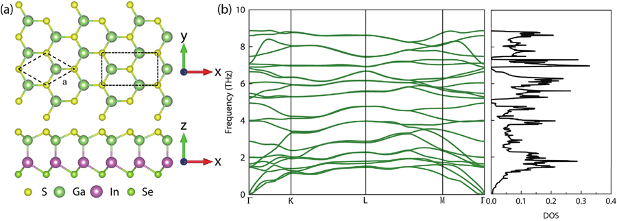
Figure 1.(Color online) (a) Top and side views of atomic structure of the Janus InGaSSe monolayer. The yellow, light green, purple and green balls represent S, Ga, In and Se atoms, respectively. (b) Phonon dispersions (left-hand) and corresponding projected density of states (right-hand) of the Janus InGaSSe monolayer.
whereESis the total strain energy of each atomic structure subjected to the respective strain component
. Here the strain
was applied according to the Cauchy-born rule[37]. For example, the new atomic positionxi subjected to a strain state was initialized according to
, whereXi represents atomic position under stress-free state andi denotes the strain direction. The elastic moduli were then extracted by fitting the strain energy with respect to associated strain component according to Eq. (1). It should be noted that the Voigt notation is adopted hereafter (i.e., 1 denotesxx, 2 denotesyy and 6 denotesxy). Once the elastic moduli are obtained, the Young’s modulusE and the Poisson ratiov may be immediately evaluated through Eqs. (2) and (3):
The structural stability of the hypothesized Janus InGaSSe monolayer can be evaluated in terms of Born’s mechanical stability[38]; that is,C11,C22,C66 > 0 andC11C22 –C122 > 0. In addition, its dynamic stability was validated by phonon dispersions and associated density of states in absence of any imaginary band as shown inFig. 1(b). Moreover, theab initio molecular dynamics (AIMD) simulations based on canonical (NVT) ensemble were also carried out to confirm the thermodynamic stability of the Janus InGaSSe monolayer at finite temperatures. As seen from variations of total energies together with the captured atomic snapshot shown inFig. 2, the average total energy at each temperature remains almost invariant until 900 K and no obvious distortion was observed in the corresponding final atomic configuration at each temperature. Based on this evidence, one can conclude that the hypothesized Janus InGaSSe monolayer is indeed thermally stable.
Figure 2.(Color online) Total energy variation of the Janus InGaSSe monolayer with respect to AIMD simulation time at 300, 500, 700 and 900 K. The inset shows the captured snapshot of the InGaSSe monolayer at 900 K.
As can be clearly seen from the electronic band structure (Fig. 3(a)) based on GGA functional, the Janus InGaSSe monolayer shows semiconducting character with a direct band gap of 1.3 eV at Γ point. It is also revealed by the projected density of state (PDOS) that both valence band maximum (VBM) and conduction band minimum (CBM) are mainly contributed by thep-orbitals as shown in right panel ofFig. 3(a). The characteristic of electronic band structure diagram implies that the Janus InGaSSe monolayer is indeed a possible candidate for optoelectronic applications, such as a photocatalyst for water splitting. As aforementioned, the HSE06 functional usually provide more reliable electronic band structure. Therefore, for comparison purpose, electronic band structures based on both HSE06 and LDA functionals are also shown inFigs. 3(b) and3(c). It can be seen that both functionals return direct band gaps, while the gap values are in order of 2.12, 1.3 and 0.96 eV for HSE06, GGA and LDA functionals, respectively. Obviously, both GGA and LDA functionals underestimate the band gap.
Figure 3.(Color online) (a) The electronic band structure (left) and PDOS (right) of the Janus InGaSSe monolayer. (b) The electronic band structures based on HSE06 functional and (c) LDA functional. The Fermi level is set at zero and the band gap is indicated by shaded area.
Next, the planar average electrostatic potential was evaluated. As shown inFig. 4, the electrostatic potential energy difference ∆φ between S and Se layer was obtained as 3.51 eV, which indicates that a local embedded electric field can be induced and thus promotes redistribution of the charge carriers across the asymmetric atomic layers.
Figure 4.(Color online) The planar average electrostatic potential of the Janus InGaSSe monolayer along the out-of-plane direction.
It was stated that both in-plane and out-of-plane piezoelectric responses exist in such kinds of Janus monolayers owing to their broken mirror symmetric structures. Hence, the piezoelectronic coefficients were determined by linearly fitting the poplarizations with respect to a series of applied elastic strains (Fig. 5). The in-plane piezoelectronic coefficiente11 was found to be 1.9 × 10⁻¹⁰ C/m, which is smaller than that of MoSSe (3.74 × 10⁻¹⁰ C/m), MoS2 (3.06 × 10⁻¹⁰ C/m) and MoSe2 (2.80 × 10⁻¹⁰ C/m) monolayer[35,36], respectively. Meanwhile, the out-of-plane piezoelectric coefficiente31 was detemined as 0.0124 × 10⁻¹⁰ C/m, which is also smaller than that of MoSSe (0.032 × 10⁻¹⁰ C/m) monolayer[35].
Figure 5.Linear fitting of (a) the in-plane piezoelectric coefficiente11 and (b) the out-of-plane piezoelectric coefficiente31.
In general, a good photocatalyst for water splitting requires a suitable band gap, appropriate band edge positions, proper energy conversion efficiencies, a strong optical absorption coefficient, a small exciton binding energy and effective spatial distribution of carriers, and more importantly high carriers' mobility[39]. Inspired by these requirements, it is highly desired to increase the carriers' mobility so that they can move quickly to the chemically active sites. As a result, the investigation on change of carriers mobility becomes one of the key tasks in this work.
According to the definition, a few related parameters need to be determined before calculating the carriers mobility. First, the effective mass of the charge carrier can be evaluated through the following expression
where
is the energy at wave vectork,
is the reduced Planck constant andm* is the effective mass of a charge carrier in unit ofm0. Second, the deformation potentialEd can be obtained by
where
represents energy of the band edge corresponding to the associated strain state
. With this relation, the deformation potentials can be extracted for both electron and hole carriers as 6.15 and 2.52 eV, respectively (Fig. 6). Finally, the carrier mobility of Janus InGaSSe monolayer can be calculated through[40,41]:
Figure 6.The fitting curves of deformation potential constants (a) for electron carrier and (b) for hole carrier of the Janus InGaSSe monolayer.
wheree,C2D,kB andT define electron charge, the elastic modulus, the Boltzmann constant and the temperature, respectively, as listed inTable 2. Without lose generality, the temperatureT is set as 300 K in this work. Hence, both electron and hole carriers' mobility are then determined.
Table Infomation Is Not Enable
It is clearly seen that mobility of both types of charge carriers are an order of magnitude greater than those of MoSSe (MoS2) monolayer, whose values are only 73.8 (160.6) and 157.2 (2047.8) cm2/(V·s) for electron and hole carriers, respectively. This implies that the Janus InGaSSe monolayer is indeed an extraordinary candidate for photocatalyst because MoSSe and MoS2 were suggested to be fairly good photocatalysts earlier[42]. In addition, such a large carrier mobility can, to certain degree, reduce the possibilities of recombination of electrons and holes.
Finally, it is also necessary to check the optimized adsorption sites for hydrogen atoms on two faces of the Janus InGaSSe monolayer. The adsorption energy is calculated according to Eq. (7):
whereEt,EInGaSSe andEH denote total energy of the adsorbed structure, the pristine Janus InGaSSe monolayer and one isolated hydrogen atom. By comparing the adsorption energies for each possible site (seeTable 3), it is found that the site 2 and the site 4 (i.e., top-S and top-Se sites) are the most stable adsorption sites on S-face and Se-face, respectively, with larger negative values, as shown in the right-hand panel ofFig. 7. Meanwhile, the changes of the Gibbs free energy for hydrogen adsorption on two faces of InGaSSe monolayer were also calculated in terms of
Table Infomation Is Not Enable
Figure 7.(Color online) The changes of Gibbs free energy (∆GH) for hydrogen adsorption with respect to different adsorption sites (left-hand panel); The possible hydrogen adsorption sites on S-face and Se-face of the Janus InGaSSe monolayer as indicated by the numbers (right-hand panel).
where ∆EH, ∆EZPE and ∆SH denote the total energy difference between adsorbed system and isolated hydrogen atom and the pristine InGaSSe monolayer, difference of the zero-point energy and the difference of entropy for the hydrogen atom between its adsorbed states and isolated states. The temperatureT was taken as 298.15 K. As shown in the left-hand panel ofFig. 7, the H-adsorption on top-S site and top-Se sites results in relatively larger negative ∆GH,which implies that the adsorption process can be spontaneous. Furthermore it also indicates that desorption of hydrogen atom on these sites is difficult, which is attributed to the larger negative adsorption energies (Table 3). In contrast, the H-adsorption on site 3 and site 6 possesses much smaller negative values of ∆GH, implying top-Ga and top-In are more active sites on two faces respectively. In particular, top-In can be the best catalytic site since the change of Gibbs free energy of this site is closer to zero and it has higher hydrogen adsorption energy.
Strain effect on transport properties
As already having been demonstrated by a large number of pioneer works, the elastic strain shows substantial effects on the electronic related properties of semiconducting materials, such as C568[29], TMDs[43] and many others[44]. Therefore, in this section, the strain effect on electronic properties of the Janus InGaSSe monolayer is also of particular interest.
First, the electronic band structure of the Janus InGaSSe monolayer under each elastic strain state was calculated. It is found that both uniaxial and biaxial strains reduce band gap values. In other words, the intrinsic stress-free Janus InGaSSe monolayer achieves maximum band gap, which implies that its residual stress should be completely relaxed to obtain the largest band gap. More importantly, the direct-to-indirect band transition behavior occurs at about 4% in uniaxial tension while it occurs at about 2% in biaxial tension (Fig. 8(a)). To further evaluate the strain effect on the band edge positions, the explicit band structures of Janus InGaSSe monolayer under strain states are also shown inFigs. 8(b) and8(c). It is seen that under either uniaxial strain or biaxial strain states, the VBM raises as strain increasing, while the CBM shifts down as strain increases.
Figure 8.(Color online) (a) The dependence of electronic band gap values on both uniaxial and biaxial strains. (b) Band structures of the Janus InGaSSe monolayer under uniaxial strains. (c) Band structures of the Janus InGaSSe monolayer under biaxial strains. The arrows indicate the positions of CBM and VBM for each case.
Second, the strain effects on the electrostatic potential difference between S and Se atomic layers were also explored. As shown inFig. 9, the electrostatic potential difference ∆φ decreases almost linearly with respect to both uniaxial and biaxial strains. Thereinto, biaxial strain shows larger effect on the changes of electrostatic potential difference, which can be illustrated by a larger slope.
Figure 9.(Color online) Dependence of electrostatic potential difference of the Janus InGaSSe monolayer on uniaxial and biaxial strains.
FromFig. 10(a), it can be seen that the electron carrier mobility shows very slight oscillation behavior under strain range between –4% and 8%, while it dropped substantially when larger compression is applied. It should be emphasized that it possesses a very small band gap under such a large compression state (seeFig. 8(a)), which is already not an ideal state for optoelectronic application. Meanwhile, the hole carrier mobility does not show obvious dependence on biaxial strain as shown by red curve inFig. 10(b). In contrast, when uniaxial compressive strain is applied, it becomes almost 10 times larger than that under the stress-free and uniaxial tension states. These dependencies show that both uniaxial and biaxial strain can tune the carriers mobility.
Figure 10.(Color online) (a) Mobility of electron carriers and (b) hole carriers of the Janus InGaSSe monolayer under both uniaxial and biaxial strains.
In summary, the electromechanical and charge transport properties of a novel hypothesized Janus InGaSSe monolayer have been extensively explored by means of first-principles calculations. It is found that the Janus InGaSSe monolayer is an excellent candidate for photocatalytic water splitting due to its extraordinary optoelectronic and electromechanical properties. In addition, both deformation potential and electrostatic potential difference decrease with respect to the applied strains. More importantly, it is shown that the hole carrier mobility can be significantly enhanced by applying uniaxial compression, while it does not change much when subjected to uniaxial tension. In contrast, the electron carrier mobility decreases when uniaxial or biaxial compression is larger than 4%, while it does not response sensitively to the tensile strain. Our results provide valuable guidance for manipulating the electronic and photoelectronic properties of the Janus 2D materials.
Li Zhong, Xiaobao Li, Wei Wang, Xinle Xiao. Electromechanical and photoelectric properties of a novel semiconducting Janus InGaSSe monolayer[J]. Journal of Semiconductors, 2023, 44(1): 012701