
Gang CHEN, Ding-Quan LIU, Chong MA, Kai-Xuan WANG, Li ZHANG, Ling-Shan GAO. Spectrum modulation of a thin-film filter with visible and near infrared dual band-pass channel [J]. Journal of Infrared and Millimeter Waves, 2020, 39(6): 791
- Journal of Infrared and Millimeter Waves
- Vol. 39, Issue 6, 791 (2020)
Abstract
Key wards: optical thin film, dual spectrum channel filter, ion beam sputtering deposition, spectrum modulation
引言
在利用可见光波段遥感成像的同时让激光回波被相机同步感知,就可以实现空间对地物目标的三维立体成像[
基于各层薄膜之间界面上形成的前向子波的干涉,经过滤光片的透射波在某些波段出现干涉增强,在另外一些波段干涉减弱。将干涉增强波段设计在需要透射的工作光谱区域,把干涉减弱的波段设计在需要抑制的其他光谱区。这样就可以利用工作光谱对目标进行观测成像,抑制背景光和杂散光,有利于提高成像质量和观测准确性。在本文研究工作中,希望可见光波段的透过率尽可能高,同时将近红外激光探测波段的峰值透过率控制在25%~28%范围,相机自身发出的探测激光回波信号的能量够用又不会饱和。
1 薄膜设计
在可见光和近红外光谱区域,熔石英是非常好的透光材料[
由于可见光波段的透射光谱较宽,要求通带边缘的光谱变化迅速,在薄膜设计的时候,采用了短波截止滤光(长波通)膜系和长波截止滤光(短波通)膜系相结合的方法,形成可见光工作波段的光谱通带。长波通膜系在长波方向一般没有高级次的反射带[
长波通膜系的设计为:Sub//0.563H 0.79L 1.554H 0.598L 0.863H 4.691L (0.563H 1.074L 0.563H)^110.359H 1.195L 0.712H 2.265L (1.52L 3.188H 1.52L)^11 1.038L 0.412H 0.46L 1.352H 1.595L//Air。其中,Sub和Air分别代表基片和空气,H和L分别代表光学厚度为设计波长1/4的高折射率(Ta2O5)膜层和低折射率(SiO2)膜层,这里的设计波长λ1=400 nm。这一膜系的透过率曲线如图1所示。
![]()
Figure 1.Transmittance curve of the designed long-pass filter
短波通膜系的设计为:Air//0.725L 1.768H 0.233L 0.499H 0.195L 2.904H 1.312L(1.16H 1.16L)^111.16H 1.265L 2.516H 1.206L 0.994H 0.595L(.5L 1H.5L)^11 0.588L 1.02H 1.186L 1.476H 0.053L 1.171H 0.267L 0.163H//Sub,这里的设计波长λ2=800 nm。这一膜系的透过率曲线如图2所示。
![]()
Figure 2.Transmittance curve of the designed short-pass filter
从图1和2可以看出,长波通膜系和短波通膜系的结合形成了一个500~720 nm的光谱带通。在波长1 064 nm附近长波通膜系和短波通膜系均有一个透射峰,这两个透射峰并不完全重合,交叠之后在1 064 nm波长处形成一个透过率小于30%的透射峰。由于1 064 nm波长处的这个合成透射峰受到两个膜系的共同影响,其通带的宽度和透过率都难以控制,因此将这一透射峰的形成改为由短波通膜系单独实现,改进后的长波通膜系和短波通膜系如图3和图4所示。图4中右侧,位于波长1 064 nm处的透射峰由一个膜系单独形成,该透射峰的波长位置、通带宽度、透过率等均易于控制。
![]()
Figure 3.Transmittance curve of the designed long-pass filter after improving
![]()
Figure 4.Transmittance curve of the designed short-pass filter after improving
改进后的短波通膜系为:Air//0.488L 0.97H 1.029L (……隐去平滑修饰膜层4层……)1.04H 0.350L 0.242H 0.154L 0.881H 1.210L 1.243H 1.194L 1.044H 1.042L 1.051H 1.194L 1.198H 1.114L 0.951H 1.013L 0.929H
![]()
Figure 5.Transmittance curve of the designed dual band-pass filter after improving
2 膜层厚度误差对光谱的影响
对优化后的短波通膜系,利用OptiLayer软件进行了膜层误差对于光谱的敏感度分析,各个膜层的敏感度分布在图6中给出。这些膜层的敏感程度差异较大,最为敏感的是(从基片算起)第28层膜,其次为第26层膜,他们都是标记为1.161L的低折射率膜层。通常情况下,控制住最为敏感的几层膜是复杂膜系制备中的关键环节[
![]()
Figure 6.Sensitivity distributing column of each layers of the short-pass filter
对整个膜系结构中最敏感的第28层引入1~3%的误差,观察这样的误差对透射率光谱曲线的影响。发现引入误差对500~720 nm可见光工作波段的影响可以忽略,但是对波长1 064 nm处的透射峰影响明显,引入误差对光谱的影响在图7-8中给出。从图8可以看出,哪怕只引入1%的误差,该透射峰就会偏离工作波长,因此该层薄膜的误差应该在0.5%以内,对应于0.9 nm的几何厚度。本文使用的双离子束溅射薄膜制备系统,能够有效控制膜层几何厚度0.5 nm以内,保证了所设计的复杂光学膜系的有效制备。
![]()
Figure 7.Influence of layer thickness error on the transmittance curve of the designed short-pass filter after improving
![]()
Figure 8.Influence of layer thickness error on the 1064nm transmission peak curves
3 滤光片的制作
薄膜的制备采用双离子束溅射沉积(Dual Ion Beam Sputtering,DIBS)技术。双离子束溅射沉积技术,是一种经典的精密光学薄膜制备方法[
![]()
Figure 9.Schematic layout of the DIBS thin films fabrication system
![]()
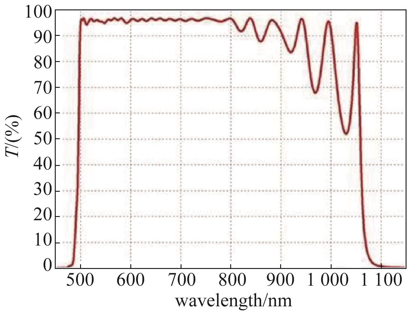
Figure 10.Transmittance curves of the dual band-pass filter
4 结论
利用长波通和短波通结合的光学膜系,在波长500~720 nm的可见光工作波段形成了矩形度很好的光谱通带,波形系数接近1.13;通过对短波通膜系的优化,在波长1 064 nm处形成一个透过率为26%左右的透射峰,用于光学系统的激光透射。这样,就在滤光片的任一几何位置上同时得到了可见光和近红外的双光谱带通。近红外光谱带通对膜层的误差非常敏感,敏感层的厚度误差需要控制在0.9 nm以内。采用双离子束溅射沉积技术制备了所有薄膜,实际膜层误差控制在0.5 nm以内,测量得到的可见光和近红外双带通薄膜滤光片透射光谱曲线与设计曲线基本吻合。
References
[1] A W Yu, M A Krainak, D J Harding. 2. Proc. of SPIE, 8599, 85990(2013).
[2] M A Krainak, J B Abshire, J Camp. 3. Proc. of SPIE, 8381, 83810(2012).
[4] HJ Li, HJ He, JC Yu. Dual-band simultaneous lasing in MOFs single crystals with Fabry-Perot microcavities. Science China Chemistry, 62, 987-993(2019).
[6] H A Macleod. Thin-film optical filters, 279(2010).
[7] J R Oh, S H Cho, H K Park. Full down-conversion of amber-emitting phosphor-converted light-emitting diodes with powder phosphors and a long-wave pass filter. Optics Express, 18, 11063-11072(2010).
[8] S A Kumar, C L Nagendra, H G Shanbhogue. Near-infrared bandpass filters from Si/SiO2 multilayer coatings. Optical Engineering, 38, 368-380(1999).
[11] . Effect of annealing on the damage threshold and optical properties of HfO2/Ta2O5/SiO2 high-reflection film. Chinese Optics Letters, 17, 113101(2019).
[14] Third-order nonlinear optical properties of WTe2 films synthesized by pulsed laser deposition. Photonics Research, 7, 12001493(2019).
[15] E K Ejigu, B M Lacquet. Sensitivity versus polarisation in multilayer optical thin film design. S Afr J Sci, 108, 7-8(2012).
[16] Film thickness measurement based on nonlinear phase analysis using a Linnik microscopic white-light spectral interferometer. Applied Optics, 57, 2955-2961(2018).
[17] J Y Wu, C Lee. Effect of the working gas of the ion-assisted source on the optical and mechanical properties of SiO2 films deposited by dual ion beam sputtering with Si and SiO2 as the starting materials. Applied Optics, 45, 3510-3515(2006).
[18] C Lee, C J Tang. TiO2-Ta2O5 composite thin films deposited by radio frequency ion-beam sputtering. Applied Optics, 45, 9125-9131(2006).
[20] J Yang, X K Weng, M L Zhang. The effects of interruption time on the growth of Ge islands prepared by ion beam sputtering deposition. Vacuum, 154, 115-119(2018).

Set citation alerts for the article
Please enter your email address
© Copyright 2018-2021 | Chinese Laser Press. All Rights Reserved 沪ICP备15018463号-20