• Chinese Optics Letters
  • Vol. 21, Issue 4, 041605 (2023)
Baizhong Li1、2, Pengkun Li1、2, Lu Zhang1、2, Ruifeng Tian1、2, Qinglin Sai1, Mingyan Pan1, Bin Wang1, Duanyang Chen1, Youchen Liu1, Changtai Xia1, and Hongji Qi1、3、*
Author Affiliations
  • 1Key Laboratory of Materials for High Power Laser, Shanghai Institute of Optics and Fine Mechanics, Chinese Academy of Sciences, Shanghai 201800, China
  • 2Center of Materials Science and Optoelectronics Engineering, University of Chinese Academy of Sciences, Beijing 100049, China
  • 3Hangzhou Institute of Optics and Fine Mechanics, Hangzhou 311421, China
  • show less
    DOI: 10.3788/COL202321.041605 Cite this Article Set citation alerts
    Baizhong Li, Pengkun Li, Lu Zhang, Ruifeng Tian, Qinglin Sai, Mingyan Pan, Bin Wang, Duanyang Chen, Youchen Liu, Changtai Xia, Hongji Qi. Optical and electrical properties of Sb-doped β-Ga2O3 crystals grown by OFZ method[J]. Chinese Optics Letters, 2023, 21(4): 041605 Copy Citation Text show less
    Photos of the as grown Sb-doped β-Ga2O3 crystals. (a) 0.1% Sb; (b) 1.0% Sb; (c) 2.0% Sb.
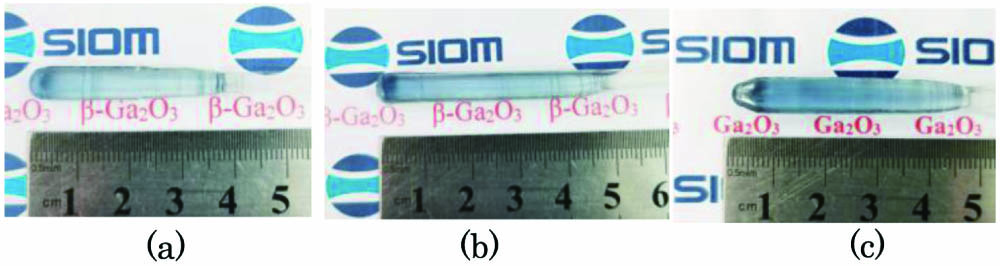
    Fig. 1. Photos of the as grown Sb-doped β-Ga2O3 crystals. (a) 0.1% Sb; (b) 1.0% Sb; (c) 2.0% Sb.
    XRD patterns of the database (PDF: 41-1103) and Sb-doped β-Ga2O3 single crystals.
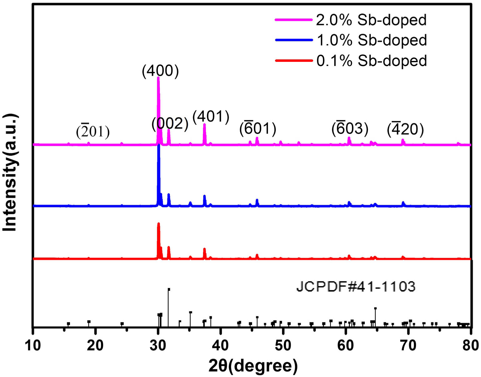
    Fig. 2. XRD patterns of the database (PDF: 41-1103) and Sb-doped β-Ga2O3 single crystals.
    X-ray rocking curve for the (400) plane of 1.0% Sb-doped β-Ga2O3 single crystal.
    Fig. 3. X-ray rocking curve for the (400) plane of 1.0% Sb-doped β-Ga2O3 single crystal.
    Room temperature Raman spectra of Sb-doped β-Ga2O3 single crystals.
    Fig. 4. Room temperature Raman spectra of Sb-doped β-Ga2O3 single crystals.
    Room temperature Raman spectra of Sb-doped β-Ga2O3 single crystals in the 300–460 cm−1 wavenumber range.
    Fig. 5. Room temperature Raman spectra of Sb-doped β-Ga2O3 single crystals in the 300–460 cm−1 wavenumber range.
    Optical transmittance of un-doped and Sb-doped β-Ga2O3 crystals. (a) 200–2000 nm (including their carrier concentrations), (b) 250–300 nm.
    Fig. 6. Optical transmittance of un-doped and Sb-doped β-Ga2O3 crystals. (a) 200–2000 nm (including their carrier concentrations), (b) 250–300 nm.
     Sample 1Sample 2Sample 3
    Nominal composition Sb (%)0.11.02.0
    Rod [ICP-AES (%)]0.01420.02060.0309
    Crystal [ICP-AES (%)]0.01010.01570.0237
    Effective segregation coefficient0.710.760.77
    Table 1. ICP-AES Data of Sb-Doped β-Ga2O3 Crystals with Different Sb Doping Concentrations
    SamplesCarrier TypeCarrier Concentration (cm−3)Mobility (cm2 · V−1 · s−1)Resistivity (Ω · cm)
    β-Ga2O3n9.55×1016153.10.603
    β-Ga2O3:Sb (0.1%)n5.40×1017134.70.064
    β-Ga2O3:Sb (1%)n1.54×1018126.40.037
    β-Ga2O3:Sb (2%)n8.10×1018108.70.017
    Table 2. Room-Temperature Hall Data of the Un-Doped and Sb-Doped β-Ga2O3 Crystals
    Baizhong Li, Pengkun Li, Lu Zhang, Ruifeng Tian, Qinglin Sai, Mingyan Pan, Bin Wang, Duanyang Chen, Youchen Liu, Changtai Xia, Hongji Qi. Optical and electrical properties of Sb-doped β-Ga2O3 crystals grown by OFZ method[J]. Chinese Optics Letters, 2023, 21(4): 041605
    Download Citation