• Journal of Semiconductors
  • Vol. 40, Issue 4, 041901 (2019)
Haizhen Wang1、2, Chen Fang1, Hongmei Luo2, and Dehui Li1
Author Affiliations
  • 1School of Optical and Electronic Information and Wuhan National Laboratory for Optoelectronics, Huazhong University of Science and Technology, Wuhan 430074, China
  • 2Department of Chemical and Materials Engineering, New Mexico State University, Las Cruces, NM 88003, United States of America
  • show less
    DOI: 10.1088/1674-4926/40/4/041901 Cite this Article
    Haizhen Wang, Chen Fang, Hongmei Luo, Dehui Li. Recent progress of the optoelectronic properties of 2D Ruddlesden-Popper perovskites[J]. Journal of Semiconductors, 2019, 40(4): 041901 Copy Citation Text show less

    Abstract

    Two-dimensional (2D) hybrid organic-inorganic perovskites have recently attracted attention due to their layered nature, naturally formed quantum well structure, large exciton binding energy and especially better long-term environmental stability compared with their three-dimensional (3D) counterparts. In this report, we present a brief overview of the recent progress of the optoelectronic applications in 2D perovskites. The layer number dependent physical properties of 2D perovskites will first be introduced and then the different synthetic approaches to achieve 2D perovskites with different morphologies will be discussed. The optical, optoelectronic properties and self-trapped states in 2D perovskites will be described, which are indispensable for designing the new device structures with novel functionalities and improving the device performance. Subsequently, a brief summary of the advantages and the current research status of the 2D perovskite-based heterostructures will be illustrated. Finally, a perspective of 2D perovskite materials is given toward their material synthesis and novel device applications.

    1. Introduction

    Originally, the word ‘perovskite’ originally described a mineral calcium titanate (CaTiO3) that was discovered in the Ural Mountains of Russia and named after Russian mineralogist Lev Perovski[1, 2]. Later, the term ‘perovskite’ came to represent a broad class of crystalline materials with the same structure as CaTiO3, usually denoted as formula ABX3, in which A and B are cations and X is anion[14]. Three-dimensional (3D) hybrid organic-inorganic perovskites (denoted as 3D-HOIPs) are a subclass of ABX3 materials, in which A is replaced by a monovalent organic cation[5, 6]. The synthesis of 3D-HOIPs can be traced back to as early as 1882 and the investigations on their optoelectronic properties was started around the year 1979 by Weber and his co-workers[7, 8]. Recently, due to their extraordinary performance in solar cells, 3D-HOIPs have attracted intensive interest as one of the most promising materials for high efficiency and low-cost solution processable optoelectronic applications[9, 10]. The first 3D-HOIPs based solar cell was reported in 2009, which has a power conversion efficiency (PCE) of only 3.8%[11]. Within less than 10 years, the power conversion efficiency soared to a certified efficiency of more than 20% benefiting from the high optical absorption coefficient, moderate charge mobility and very long diffusion length of 3D-HOIPs[1215]. Monolithic tandem c-Si/3D-HOIP solar cells have achieved an even higher PCE of 25% with a potential of above 30%[16]. In addition to their applications in solar cells, 3D-HOIP-based light emitting devices, lasers and photodetectors have also been demonstrated with fairly decent performance. Consequently, the 3D-HOIPs are a family of highly promising materials for diverse optoelectronic applications[1722].

    Despite the rapid advancements of 3D-HOIP-based optoelectronic applications, a number of challenges remain including hysteresis, instability and toxicity[2326]. The HOIP-based photovoltaic devices are typically plagued with considerable hysteresis in current–voltage curves, which impedes precise evaluation of the PCE and is fundamentally associated with instability in the device[27, 28]. In particular, 3D-HOIPs are not only very sensitive to moisture and oxygen in ambient environment and thus tend to undergo rapid degradation in air, but they also show degradation under thermal annealing or light illumination, which has stimulated extensive research on looking for alternatives to deal with this stability issue[2931].

    One alternative way to address the stability of 3D-HOIPs is to introduce their two-dimensional (2D) counterparts, which have attracted attention largely due to their better environmental stability[3239]. The general chemical formula for 2D perovskites can be written as R2An–1MnX3n+1, where R is long chain spacer cation, A is organic cation while X is a halide anion, M is a divalent metal and n is an integer which represents the number of [PbX6]4– octahedral sheets sandwiched between two layers of R spacer cations[34, 35, 40]. The hydrophobicity of the long organic chain R prevents [PbX6]4- octahedral sheets from being directly contacted by the moisture in air and thus the environmental stability of 2D perovskites is able to be significantly improved when compared with their 3D counterparts[32, 35]. The alternating stacked organic and inorganic layers make 2D perovskites natural quantum well structures while the weak Van de Waals coupling between organic and inorganic layers equips 2D perovskites with layered characteristic, which allows us to mechanically exfoliate thin flakes from their respective bulk crystals to integrate with other layered materials[38]. Additionally, the small dielectric constant of organic layers introduce dielectric confinement that leads to the extreme large exciton binding energy, which would be beneficial to the polaritonic devices[33, 35, 41]. In particular, the optical properties can be readily tuned by changing the layer number n and chemical compositions, endowing 2D perovskites with great flexibility for various optoelectronic applications[33, 4246].

    In this report, we will give a brief summary on the recent progress of optoelectronic properties of 2D perovskites. We will start with an introduction of the layer number n dependent environmental stability and the various methods to synthesize 2D perovskites. The optical and optoelectronic properties and self-trapped states in 2D perovskites will then be discussed. Subsequently, the growth of heterostructures based on 2D perovskites together with their optical and optoelectronic properties will be given. Finally, the outlook of 2D perovskite-based optoelectronic devices will be discussed, which will provide researchers with new insights into the future research direction regarding 2D perovskites.

    2. Varying the layer number n and the stability of 2D perovskites

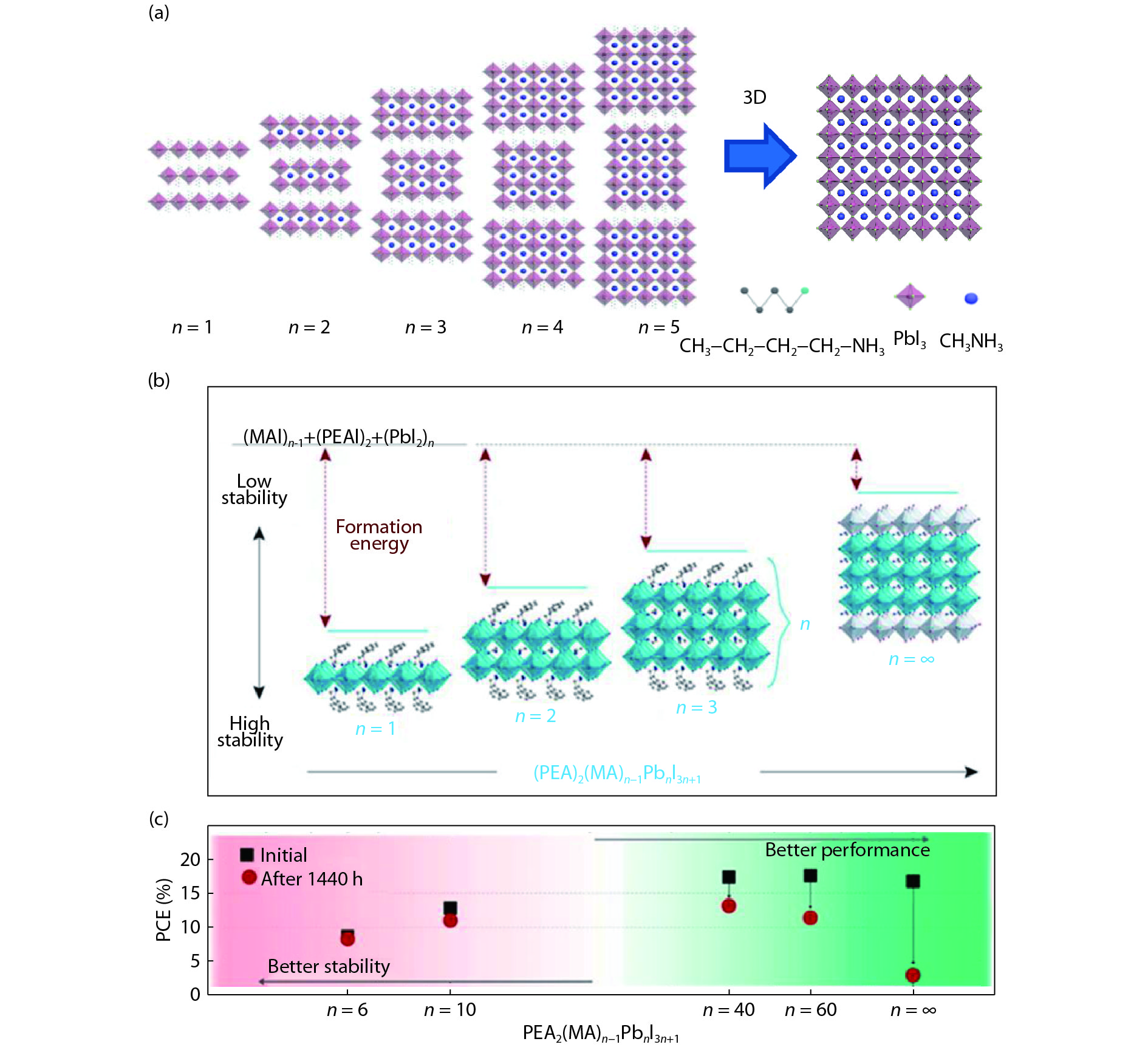
    The 2D perovskites can be viewed as the 3D perovskite frameworks being sliced into 2D slabs by the long chain organic spacer chains (Fig. 1(a))[38]. By properly tuning the stoichiometry of R to A, 2D perovskites with different layer number n can be synthesized as required, resulting in different optical, electronic and optoelectronic properties among these 2D perovskites (which will be discussed later on). As the layer number n gradually increases, the perovskites transit from pure 2D to 2D: 3D mixtures and eventually 3D when the layer number n approaches infinity (Fig. 1(a))[35, 40]. Besides, largely due to the hydrophobicity of the long organic chain R, the environmental stability of 2D perovskites can be significantly improved compared with that of 3D perovskites[32, 47]. In particular, the formation energy of 2D perovskites decreases with the increase of the layer number n, resulting in the enhanced environmental stability of 2D perovskites with the decrease of the layer number n (Fig. 1(b))[40, 4851]. This has been experimentally demonstrated in 2D perovskite-based solar cells, where the stability of the solar cells gradually increases with the layer number decreasing from infinite to 1 (Fig. 1(c))[40, 50]. For instance, it has demonstrated that the 2D perovskite-based solar cells can maintain 60% of their initial PCE under illumination after 2250 hours and show a greater moisture tolerance under 65% relative humidity[52]. In particular, Sn-based 2D perovskites also exhibit much better environmental stability compared with their 3D counterparts, which cannot be prepared in air[53]. In contrast, Sn-based 2D perovskites can be synthesized in ambient condition and the Sn-based 2D perovskite electronic devices without any encapsulation only exhibit slightly degradation in air after several hours[53].

    (Color online) (a) The schematic illustration of the crystal structures of 2D perovskite (BA)2(MA)n−1PbnI3n+1 for n = 1 to ∞. (b) The structure schematic illustration and stability of 2D perovskite (PEA)2MAn−1PbnI3n+1 for n = 1 to ∞. (c) The layer number n-dependent power conversion efficiency as well as device performance and stability of (PEA)2MAn−1PbnI3n+1. Panel (a) adapted with permission from Ref. [38]. Copyright 2018, Institute of Physics (Great Britain). Panels (b) and (c) adapted with permission from Ref. [50]. Copyright 2016, American Chemical Society.

    Figure 1.(Color online) (a) The schematic illustration of the crystal structures of 2D perovskite (BA)2(MA)n−1PbnI3n+1 for n = 1 to ∞. (b) The structure schematic illustration and stability of 2D perovskite (PEA)2MAn−1PbnI3n+1 for n = 1 to ∞. (c) The layer number n-dependent power conversion efficiency as well as device performance and stability of (PEA)2MAn−1PbnI3n+1. Panel (a) adapted with permission from Ref. [38]. Copyright 2018, Institute of Physics (Great Britain). Panels (b) and (c) adapted with permission from Ref. [50]. Copyright 2016, American Chemical Society.

    Nevertheless, the presence of the long chain spacer cations among inorganic layers would introduce barriers for the carriers to transport across the organic layers, inducing a huge resistivity in the out-of-plane direction[54, 55]. Consequently, the photogenerated carriers cannot be efficiently extracted, which leads to a low PCE in the pure 2D perovskite-based solar cells (Fig. 1(c))[33, 40, 52]. The highest PCE of the pure 2D perovskite-based solar cells is over 10%, much lower than that of 3D perovskite based solar cells[52]. Therefore, there is a trade-off between the stability and the device performance in HOIP-based photovoltaic devices. To compromise those two factors, 2D:3D mixed perovskites have been introduced that possess the good charge transport property of 3D perovskites without sacrificing too much of the environmental stability by inheriting the excellent stability of 2D perovskites[5658]. Thus, the 2D:3D mixed perovskite-based solar cells and other optoelectronic devices exhibit fairly good performance and great environmental stability[5961].

    3. The synthesis of 2D perovskites

    Recently, a number of growth methods have been developed to synthesize 2D perovskites with various compositions and morphologies. While 2D perovskite crystals of hundreds of micrometers size have been prepared by a solution method to study their crystal structure, optical properties and band structures (Fig. 2(a))[35], a template-assisted synthesis approach has recently been used to obtain very thin millimeter-size plates for photodetections[62]. In terms of the photovoltaic applications, large-scale 2D perovskite thin films have been successfully synthesized by a spin-coating method with rather smooth surface and different colors for different layer number n, suggesting the change of the band gap[40, 63]. Nevertheless, it is usually difficult to obtain pure phase 2D perovskite crystals or films with all those synthetic methods due to the similar thermodynamics for the chemical reaction[38].

    (Color online) (a) Scanning electron microscopy (SEM) images of (BA)2(MA)n−1PbnI3n+1 perovskite crystals. The scale bars are 200 μm. (b) Photographs of (BA)2(MA)n−1PbnI3n+1 perovskite films. (c) Optical microscopy (OM) images of the as-exfoliated (BA)2(MA)n−1PbnI3n+1 perovskite microplates. The scale bars are 15 μm. (d) OM image of (BA)2PbBr4 square microplates grown on Si substrate via a solution-phase growth method. The scale bar is 10 μm. (e) OM image of (BA)2(MA)Pb2I7 square plates grown on Si substrate via a spin-coating method. The scale bar is 5 μm. (f) OM image of (BA)2PbI4 flakes grown on mica substrate via a co-evaporation method. The scale bar is 5 μm. (g) OM image of the converted (BA)2Pbl4−xClx microplate array on Si via a vapor phase intercalation method. The scale bar is 20 μm. Panel (a) adapted with permission from Ref. [33]. Copyright 2016, American Chemical Society. Panel (b) adapted with permission from Ref. [40]. Copyright 2015, American Chemical Society. Panel (d) adapted with permission from Ref. [67]. Copyright 2015, The American Association for the Advancement of Science. Panel (e) adapted with permission from Ref. [68]. Copyright 2018, Royal Society of Chemistry (Great Britain). Panel (f) adapted with permission from Ref. [69]. Copyright 2017, John Wiley and Sons. Panel (g) adapted with permission from Ref. [70]. Copyright 2018, American Chemical Society.

    Figure 2.(Color online) (a) Scanning electron microscopy (SEM) images of (BA)2(MA)n−1PbnI3n+1 perovskite crystals. The scale bars are 200 μm. (b) Photographs of (BA)2(MA)n−1PbnI3n+1 perovskite films. (c) Optical microscopy (OM) images of the as-exfoliated (BA)2(MA)n−1PbnI3n+1 perovskite microplates. The scale bars are 15 μm. (d) OM image of (BA)2PbBr4 square microplates grown on Si substrate via a solution-phase growth method. The scale bar is 10 μm. (e) OM image of (BA)2(MA)Pb2I7 square plates grown on Si substrate via a spin-coating method. The scale bar is 5 μm. (f) OM image of (BA)2PbI4 flakes grown on mica substrate via a co-evaporation method. The scale bar is 5 μm. (g) OM image of the converted (BA)2Pbl4−xClx microplate array on Si via a vapor phase intercalation method. The scale bar is 20 μm. Panel (a) adapted with permission from Ref. [33]. Copyright 2016, American Chemical Society. Panel (b) adapted with permission from Ref. [40]. Copyright 2015, American Chemical Society. Panel (d) adapted with permission from Ref. [67]. Copyright 2015, The American Association for the Advancement of Science. Panel (e) adapted with permission from Ref. [68]. Copyright 2018, Royal Society of Chemistry (Great Britain). Panel (f) adapted with permission from Ref. [69]. Copyright 2017, John Wiley and Sons. Panel (g) adapted with permission from Ref. [70]. Copyright 2018, American Chemical Society.

    To obtain pure phase 2D perovskites for the study of their basic optical and electronic properties, a mechanical exfoliation method was adopted to peel 2D perovskite microplates from their respective bulk crystals. Micro-absorption and power-dependent photoluminescence studies reveal that the impurity phases are physically mixed, which allows us to achieve pure phase 2D perovskite microplates via mechanical exfoliation[38, 60, 64]. It has demonstrated that pure phase 2D perovskite microplates with different layer number n from 1 to 5 could be successfully obtained by this exfoliation method as long as the thickness of the as-peeled microplates is below 20 nm, based on which the basic optical properties of the pure phase 2D perovskites have been studied (Fig. 2(c))[38]. The different colors in Fig. 2(c) for samples with different layer number n are due to the optical contrast resulting from the thickness difference of the exfoliated microplates. Thus, optical contrast is a convenient way to distinguish the thickness of the microplate, similar to the case in graphene and transition metal dichalcogenides[65].

    The 2D perovskite crystals with the desired shape might find important applications in optoelectronics and thus a series of synthetic strategies have been adopted to achieve 2D perovskites with different morphologies[66]. The atomically thin 2D perovskite microplates with square shape were successfully prepared by solution method by Peidong Yang’s group (Fig. 2(d)) while butterfly-shaped 2D (C4H9NH3)2PbI4 and square-shaped (C4H9NH3)2(CH3NH3)Pb2I7 and (C4H9NH3)2PbI4/(C4H9-NH3)2(CH3NH3)Pb2I7 microstructures were fabricated on a large scale with a simple spin-coating method (Fig. 2(e))[67, 68]. The vapor phase transport method was also used to directly grow 2D perovskite microstructures on a mica substrate (Fig. 2(f))[69]. Additionally, a two-step method combining the solution method and vapor phase transport has been developed to controllably grow 2D perovskite (C4H9NH3)2PbI4 microplates with hexagonal shape and microplate arrays to the predefined sites (Fig. 2(g))[70]. This two-step growth method allows us to directly make electronic devices and device arrays that allow further investigation of their electronic and optoelectronic properties. In particular, the Cl element can be truly incorporated into the crystal lattice by this method to improve charge transport and tune the morphology, which cannot be achieved in 3D perovskites[71].

    4. Optical and optoelectronic properties of 2D perovskites

    The naturally formed quantum well structure and large dielectric constant difference between the organic layer and inorganic layer result in the novel and interesting optical and optoelectronic properties in 2D perovskites. By changing the layer number n, the quantum confinement strength can be readily tuned and this leads to a gradual shift of both emission peak and absorption onset in a wider range of wavelength (Figs. 3(a) and 3(b))[33, 35, 38]. The large dielectric constant difference between the organic and inorganic layer leads to the extremely large exciton binding energy on the order of hundreds of meV due to the dielectric confinement[33, 40]. Furthermore, the diversity of the available organic molecules allows us to properly select the long chain spacer cation so that the dielectric constant of the organic layer and thus the exciton binding energy can be tuned[33]. This tunable and large exciton binding energy of 2D perovskites would be beneficial to their polaritonic applications[41]. Overall, the unique and excellent optical and optoelectronic properties of 2D perovskites make them attractive candidates for the optoelectronic applications including the photodetectors, lasers, light emitting devices and energy harvesting.

    (Color online) (a) Normalized PL spectra of the as-exfoliated (BA)2(MA)n−1PbnI3n+1 microplates for n = 1–5 with thickness below 20 nm. (b) Normalized absorption spectra of the as-synthesized (BA)2(MA)n−1PbnI3n+1 plates for n = 1–5. (d) The current–voltage curves of the (BA)2(MA)2Pb3I10 device in dark and under illumination with a 528-nm LED. Inset shows the schematic of the two-probe device. The incident power is 30 μW/cm2. (d) Spectral response of the graphene-(BA)2PbBr4-graphene device under a fixed incident power. The schematic of the as-fabricated device is shown in the inset. (e) Electroluminescence spectra of the (PEA)2MAn−1PbnI3n+1 perovskite films with different n values. (f) Carrier transfer process in (PEA)2MA4Pb5I16 perovskite film. (g) Energy funneling process of (PEA)2MA4Pb5I16 films. Panels (a)–(c) adapted with permission from Ref. [38]. Copyright 2018, Institute of Physics (Great Britain). Panel (d) adapted with permission from Ref. [42]. Copyright 2016, American Chemical Society. Panels (e)–(g) adapted with permission from Ref. [60]. Copyright 2016, Springer Nature.

    Figure 3.(Color online) (a) Normalized PL spectra of the as-exfoliated (BA)2(MA)n−1PbnI3n+1 microplates for n = 1–5 with thickness below 20 nm. (b) Normalized absorption spectra of the as-synthesized (BA)2(MA)n−1PbnI3n+1 plates for n = 1–5. (d) The current–voltage curves of the (BA)2(MA)2Pb3I10 device in dark and under illumination with a 528-nm LED. Inset shows the schematic of the two-probe device. The incident power is 30 μW/cm2. (d) Spectral response of the graphene-(BA)2PbBr4-graphene device under a fixed incident power. The schematic of the as-fabricated device is shown in the inset. (e) Electroluminescence spectra of the (PEA)2MAn−1PbnI3n+1 perovskite films with different n values. (f) Carrier transfer process in (PEA)2MA4Pb5I16 perovskite film. (g) Energy funneling process of (PEA)2MA4Pb5I16 films. Panels (a)–(c) adapted with permission from Ref. [38]. Copyright 2018, Institute of Physics (Great Britain). Panel (d) adapted with permission from Ref. [42]. Copyright 2016, American Chemical Society. Panels (e)–(g) adapted with permission from Ref. [60]. Copyright 2016, Springer Nature.

    The 2D perovskite-based photodetectors and light emitting devices have been demonstrated with fairly good performance. The responsivity of around 100 A/W has been achieved in pure (C4H9NH3)2PbI4 microplate devices (Fig. 3(c)) while a very high responsivity of 2100 A/W has been reported in graphene-contacted (C4H9NH3)2PbBr4 heterostructures[38, 42]. In addition, 2D single crystal plate photodetectors exhibit quite strong anisotropic electric conductivity as expected due to the barriers introduced along the out-of-plane direction[54, 55, 71]. Within the 2D perovskites with hybrid phases, the band alignment favors the photogenerated carrier separation, thus beneficial to the efficiency of the solar cells and photodetectors[64, 72]. This has been experimentally proven by the time-resolved PL studies[60, 64]. For some 2D perovskites, the band alignment would prefer to form type-1 alignment, leading to the energy funneling effect (Figs. 3(e) and 3(f)). Consequently, a light emitting device based on those types of 2D perovskites shows improved efficiency (Fig. 3(g))[60].

    5. Self-trapped states in 2D perovskites

    Strong electron-phonon interaction is present in both 3D and 2D perovskites, leading to lattice deformation. Self-trapped states are formed when carriers or excitons are localized and trapped by the lattice deformation potential. The self-trapping strongly relies on the dimensionality of the systems. Unlike 3D case where a potential barrier is present for self-trapping, there is no such barrier for one-dimensional systems and a much lower potential barrier or even no potential barrier exists in 2D systems[7375]. Therefore, the formation of self-trapped states takes place easier in 2D perovskites, which would significantly alter their optical and electronic properties[73, 7678].

    Self-trapped excitons can recombine via either radiative or nonradiative pathways depending on the long chain organic molecules and halide anions in 2D perovskites. The self-trapped excitons usually feature as broad emission peaks and a large Stokes shift when compared with exciton emission peak while the self-trapped excitons in some types of 2D perovskites at room temperature only exhibit an asymmetric line shape of PL spectrum[67, 73, 77, 79]. Multiple emission peaks far beyond the band edge have been observed in room-temperature PL spectra of atomically thin (C4H9NH3)2PbCl4 microplates, which was believed to be originated from self-trapped excitons (Fig. 4(a))[67]. In (C4H9NH3)2PbI4 and (C4H9NH3)2(CH3-NH3)Pb2I7 thin films, the room-temperature sub-band gap bleaches in the transient absorption spectra and the sub-band gap broad emission peak in PL spectra at low temperature has been attributed to the self-trapped states (Fig. 4(b))[80].

    (Color online) (a) PL spectra of different 2D hybrid perovskites: (i) (BA)2PbCl4, (ii) (BA)2PbBr4, (iii) (BA)2PbI4, (iv) (BA)2PbCl2Br2, (v) BA)2PbBr2I2 and (vi) (BA)2(MA)Pb2Br7 2D microplates and their corresponding PL images as shown in the inset. The scale bars are 2 μm for (i) to (v) and 10 μm for (vi). (b) Transient absorption spectrum of (BA)2PbI4 at room temperature. (c) PL spectra of the (PEA)2PbI4 thin film and single crystal plotted as black and blue dash line, respectively. The inset shows the spectra on a logarithmic scale. Panel (a) adapted with permission from Ref. [67]. Copyright 2015, The American Association for the Advancement of Science. Panel (b) adapted with permission from Ref. [80]. Copyright 2015, American Chemical Society. Panel (c) adapted with permission from Ref. [81]. Copyright 2016, American Chemical Society.

    Figure 4.(Color online) (a) PL spectra of different 2D hybrid perovskites: (i) (BA)2PbCl4, (ii) (BA)2PbBr4, (iii) (BA)2PbI4, (iv) (BA)2PbCl2Br2, (v) BA)2PbBr2I2 and (vi) (BA)2(MA)Pb2Br7 2D microplates and their corresponding PL images as shown in the inset. The scale bars are 2 μm for (i) to (v) and 10 μm for (vi). (b) Transient absorption spectrum of (BA)2PbI4 at room temperature. (c) PL spectra of the (PEA)2PbI4 thin film and single crystal plotted as black and blue dash line, respectively. The inset shows the spectra on a logarithmic scale. Panel (a) adapted with permission from Ref. [67]. Copyright 2015, The American Association for the Advancement of Science. Panel (b) adapted with permission from Ref. [80]. Copyright 2015, American Chemical Society. Panel (c) adapted with permission from Ref. [81]. Copyright 2016, American Chemical Society.

    The emission from self-trapped states also relies on the crystalline quality of 2D perovskites. While only one broad emission peak is present in (PEA)2PbI4 thin films, two distinct peaks are observed with a much weaker strength in (PEA)2PbI4 single crystals, which suggestes that defects can enhance the strength of the self-trapping (Fig. 4(c))[81]. Furthermore, the self-trapped states can be utilized to achieve white light emitting in nonplanar 2D perovskites and the carriers in those 2D perovskites exhibit a hopping transport behavior due to the presence of the self-trapped states[73]. Recently, enhanced self-trapped states were utilized to achieve narrowband photodetections in the entire visible wavelength range with greatly improved performance[78]. Therefore, the formation of the self-trapping states could greatly alter the electrical and optical properties of the 2D perovskites and thus the performance of the optoelectronic devices based on 2D perovskites.

    6. 2D perovskite based heterostructures

    The layered nature and rather different electronic band structures of 2D perovskite series (different layer number n) suggest that it is possible to conveniently fabricate heterostructures consisting of 2D perovskites with different layer number n and the functional devices can be achieved with extended functionalities in these 2D perovskite-based heterostructures[8184]. Heterostructures have important relevance to all modern electronic and optoelectronic devices, including transistors, light emitting diodes and laser diodes. The diversity of the available organic cations in 2D perovskites allows us to flexibly select the right 2D perovskites to form heterostructures for the desired functionalities, which thus can greatly extend the material properties for electronic and optoelectronic applications.

    Both lateral and vertical (C4H9NH3)2PbI4/(C4H9NH3)2(CH3-NH3)Pb2I7 heterostructures have been grown by combining the solution method and vapor phase transport method[84]. Centimeter-size (C4H9NH3)2PbI4 crystals were first synthesized by a solution method and then portion of (C4H9NH3)2PbI4 crystals were converted to (C4H9NH3)2(CH3NH3)Pb2I7 by vapor phase intercalation to form (C4H9NH3)2PbI4/(C4H9NH3)2(CH3NH3)-Pb2I7 heterostructures (Fig. 5(a))[84]. The striking color difference before and after vapor phase intercalation confirms the conversion of (C4H9NH3)2PbI4 crystals and formation of (C4H9NH3)2-PbI4/(C4H9NH3)2(CH3NH3)Pb2I7 heterostructures (Figs. 5(b)5(d)). A scanning electron microscopy image shows that the local surface of the heterostructure is rather smooth, which would be beneficial to fabricate the electronic and optoelectronic devices (Fig. 5(e)). The formation of heterostructures was further confirmed by absorption and PL spectra for both vertical and lateral heterostructures (Figs. 5(f)5(g)). Electrical measurements have revealed that the as-synthesized heterostructures exhibit an excellent diode behavior and photoresponse (Figs. 5(h)5(i)).

    (Color online) (a) Schematic illustrations of crystal structure of (BA)2PbI4/(BA)2MAPb2I7 lateral and vertical heterostructures. (b, c) Photographs of the (BA)2PbI4/(BA)2MAPb2I7 lateral and vertical heterostructures, respectively. The boundary of lateral heterostructure are shown in Fig. 5(b) plotted as dotted line, whereas the yellow color portion represents (BA)2PbI4 and the red color portion represents (BA)2MAPb2I7 2D perovskites. (d) OM image of the (BA)2PbI4/(BA)2MAPb2I7 lateral heterostructure. Scale bar: 20 μm. (e) SEM image of (BA)2PbI4/(BA)2MAPb2I7 lateral heterostructure. Scale bar: 30 μm. Inset: the magnified SEM image with a scale bar of 3 μm. (f, g) Normalized absorption and PL spectra of (BA)2PbI4/(BA)2MAPb2I7 vertical and lateral heterostructures, respectively. (h, i) I–V curves of the (BA)2PbI4/(BA)2MAPb2I7 lateral and vertical heterostructure devices in dark and under 1.4 mW/cm2 white light illumination. Adapted with permission from Ref. [84]. Copyright 2017, American Chemical Society.

    Figure 5.(Color online) (a) Schematic illustrations of crystal structure of (BA)2PbI4/(BA)2MAPb2I7 lateral and vertical heterostructures. (b, c) Photographs of the (BA)2PbI4/(BA)2MAPb2I7 lateral and vertical heterostructures, respectively. The boundary of lateral heterostructure are shown in Fig. 5(b) plotted as dotted line, whereas the yellow color portion represents (BA)2PbI4 and the red color portion represents (BA)2MAPb2I7 2D perovskites. (d) OM image of the (BA)2PbI4/(BA)2MAPb2I7 lateral heterostructure. Scale bar: 20 μm. (e) SEM image of (BA)2PbI4/(BA)2MAPb2I7 lateral heterostructure. Scale bar: 30 μm. Inset: the magnified SEM image with a scale bar of 3 μm. (f, g) Normalized absorption and PL spectra of (BA)2PbI4/(BA)2MAPb2I7 vertical and lateral heterostructures, respectively. (h, i) I–V curves of the (BA)2PbI4/(BA)2MAPb2I7 lateral and vertical heterostructure devices in dark and under 1.4 mW/cm2 white light illumination. Adapted with permission from Ref. [84]. Copyright 2017, American Chemical Society.

    The 2D perovskite-based heterostructures also have been synthesized on a large scale by pure solution method[62]. The thickness and the junction depth of the heterostructures can be well controlled and dual narrowband photodetections have been demonstrated based on those heterostructures. Recently, 2D perovskite multi-heterostructures consisting of different layer number 2D perovskites have been successfully fabricated by a solution method[82]. With such large-size 2D perovskite-based heterostructures and multi-heterostructures, we expect that novel electronic and optoelectronic devices with desired functionalities can be designed according to our demand thanks to the diversity of the available 2D perovskites.

    7. Summary and outlook

    In summary, we have presented an overview of the recent progress of the optoelectronic applications in 2D perovskites. The 2D perovskites with layered nature exhibit rather unique properties including the naturally formed quantum well structure, extremely large exciton binding energy, strong electron-phonon coupling and a greatly tunable of band gap by either tuning the layer number or the chemical compositions[33, 35]. All those factors mean that 2D perovskites are ideal candidates for a wide range of optoelectronic and polaritonic applications. Furthermore, the different electronic band structures of 2D perovskites with the same chemical composition but different layer number n could seamlessly form heterostructures without interfacial defects and well width fluctuation, which would be superior compared to the conventional II–IV group heterostructures[38].

    Despite the breakthroughs that have been made, several issues in 2D perovskites also need to be addressed to explore more novel and interesting applications based on 2D perovskites. First, although a series of growth strategies have been developed to synthesize 2D perovskites, it is still difficult to obtain 2D perovskites with controlled composition and structures[33]. In addition, the similar thermodynamics for the synthesis of the 2D perovskites with higher layer number n makes it difficult to achieve pure phase 2D perovskites with n > 2 [38]. Nevertheless, this is essential for investigating the basic optical and electronic properties for further optoelectronic applications. Understanding the underlying growth mechanism could help to design a new growth method but is still elusive. Consequently, it is important to understand the growth process and develop new synthetic strategies. Second, the basic optical and charge transport parameters of 2D perovskites are still limited, but are indispensable for designing the new device architecture and improving the device performance. Third, 2D perovskite-based heterostructures are absent of interfacial defects and well width fluctuation, thus we expect that these electronic and optoelectronic devices will show superior performance. Nevertheless, there is still no method to controllably fabricate these heterostructures with high quality. Finally, thanks to the diversity of the available organic molecules, incorporating the chiral organic ligands would introduce charity to 2D perovskites[85]. Those chiral 2D perovskites would have the merits of both 2D perovskites and chiral materials and thus would be a promising class of materials for next-generation spintronic devices. However, studies in this field are largely unexplored and more investigations are demanded.

    Acknowledgements

    Dehui Li acknowledges the support from NSFC (No. 61674060) and the Fundamental Research Funds for the Central Universities, HUST (Nos. 2017KFYXJJ030, 2017KFXKJC002, 2017KFXKJC003 and 2018KFYXKJC016).

    References

    [1] C Moure, O Peña. Recent advances in perovskites: processing and properties. Prog Solid State Chem, 43, 123(2015).

    [2] S Mtougui, R Khalladi, S Ziti et al. Magnetic properties of the perovskite BiFeO3: Monte Carlo simulation. Superlattice Microstruct, 123, 111(2018).

    [3] C Li, X Lu, W Ding et al. Formability of ABX3 (X = F, Cl, Br, I) halide perovskites. Acta Crystallograph B, 64, 702(2008).

    [4] A S Bhalla, R Guo, R Roy. The perovskite structure—a review of its role in ceramic science and technology. Mater Res Innov, 4, 3(2016).

    [5] W Li, Z Wang, F Deschler et al. Chemically diverse and multifunctional hybrid organic–inorganic perovskites. Nat Rev Mater, 2, 16099(2017).

    [6] B Saparov, D Mitzi. Organic–inorganic perovskites: structural versatility for functional materials design. Chem Rev, 116, 4558(2016).

    [7] T M Brenner, D A Egger, L Kronik et al. Hybrid organic–inorganic perovskites: low-cost semiconductors with intriguing charge-transport properties. Nat Rev Mater, 1, 15007(2016).

    [8]

    [9] H J Snaith. Perovskites: the emergence of a new era for low-cost, high-efficiency solar cells. J Am Chem Soc, 4, 3623(2013).

    [10] M Grätzel. The light and shade of perovskite solar cells. Nat Mater, 13, 838(2014).

    [11] A Kojima, K Teshima, Y Shirai et al. Organometal halide perovskites as visible-light sensitizers for photovoltaic cells. J Am Chem Soc, 131, 6050(2009).

    [12] D Shi, V Adinolfi, R Comin et al. Low trap-state density and long carrier diffusion in organolead trihalide perovskite single crystals. Science, 347, 519(2015).

    [13] J S Shaikh, N S Shaikh, A D Sheikh et al. Perovskite solar cells: In pursuit of efficiency and stability. Mater Des, 136, 54(2017).

    [14] M B Johnston, L M Herz. Hybrid perovskites for photovoltaics: charge-carrier recombination, diffusion, and radiative efficiencies. Accounts Chem Res, 49, 146(2015).

    [15]

    [16] K A Bush, S Manzoor, K Frohna et al. Minimizing current and voltage losses to reach 25% efficient monolithic two-terminal perovskite–silicon tandem solar cells. ACS Energy Lett, 3, 2173(2018).

    [17] P Wangyang, C Gong, G Rao et al. Recent advances in halide perovskite photodetectors based on different dimensional materials. Adv Opt Mater, 6, 1701302(2018).

    [18] L Shen, Y Fang, D Wang et al. A self-powered, sub-nanosecond-response solution-processed hybrid perovskite photodetector for time-resolved photoluminescence-lifetime detection. Adv Mater, 28, 10794(2016).

    [19] R Dong, Y Fang, J Chae et al. High-gain and low-driving-voltage photodetectors based on organolead triiodide perovskites. Adv Mater, 27, 1912(2015).

    [20] Y Fang, Q Dong, Y Shao et al. Highly narrowband perovskite single-crystal photodetectors enabled by surface-charge recombination. Nat Photon, 9, 679(2015).

    [21] G Xing, N Mathews, S S Lim et al. Low-temperature solution-processed wavelength tunable perovskites for lasing. Nat Mater, 13, 476(2014).

    [22] Z Yuan, C Zhou, Y Tian et al. One-dimensional organic lead halide perovskites with efficient bluish white-light emission. Nat Commun, 8, 14051(2017).

    [23] G Niu, X Guo, L Wang. Review of recent progress in chemical stability of perovskite solar cells. J Mater Chem, A, 3, 8970(2015).

    [24] Y Rong, L Liu, A Mei et al. Beyond efficiency: the challenge of stability in mesoscopic perovskite solar cells. Adv Energy Mater, 5, 1501066(2015).

    [25] S H Turren-Cruz, M Saliba, M T Mayer et al. Enhanced charge carrier mobility and lifetime suppress hysteresis and improve efficiency in planar perovskite solar cells. Energy Environ Sci, 11, 78(2018).

    [26] A Babayigit, A Ethirajan, M Muller et al. Toxicity of organometal halide perovskite solar cells. Nat Mater, 15, 247(2016).

    [27] H J Snaith, A Abate, J M Ball et al. Anomalous hysteresis in perovskite solar cells. J Phys Chem Lett, 5, 1511(2014).

    [28] W Tress, N Marinova, T Moehl et al. Understanding the rate-dependent J–V hysteresis, slow time component, and aging in CH3NH3PbI3 perovskite solar cells: the role of a compensated electric field. Energy Environ Sci, 8, 995(2015).

    [29] R J Sutton, G E Eperon, L Miranda et al. Bandgap-tunable cesium lead halide perovskites with high thermal stability for efficient solar cells. Adv Energy Mater, 6, 1502458(2016).

    [30] B Conings, J Drijkoningen, N Gauquelin et al. Intrinsic thermal instability of methylammonium lead trihalide perovskite. Adv Energy Mater, 5, 1500477(2015).

    [31] W Nie, J C Blancon, A J Neukirch et al. Light-activated photocurrent degradation and self-healing in perovskite solar cells. Nat Commun, 7, 11574(2016).

    [32] I C Smith, E T Hoke, D Solis-Ibarra et al. A layered hybrid perovskite solar-cell absorber with enhanced moisture stability. Angew Chem, 53, 11232(2014).

    [33] Y Chen, Y Sun, J Peng et al. 2D Ruddlesden-Popper perovskites for optoelectronics. Adv Mater, 30, 1703487(2018).

    [34] L Pedesseau, D Sapori, B Traore et al. Advances and promises of layered halide hybrid perovskite semiconductors. ACS Nano, 10, 9776(2016).

    [35] C C Stoumpos, D H Cao, D J Clark et al. Ruddlesden–Popper hybrid lead iodide perovskite 2D homologous semiconductors. Chem Mater, 28, 2852(2016).

    [36] H Shen, J Li, H Wang et al. Two-dimensional lead-free perovskite (C6H5C2H4NH3)2CsSn2I7 with high hole mobility. J Phys Chem Lett, 10, 7(2018).

    [37] C Soe, C Stoumpos, M Kepenekian et al. New type of 2D perovskites with alternating cations in the interlayer space, (C(NH2)3)(CH3NH3)nPbnI3n+1: Structure, properties, and photovoltaic performance. J Am Chem Soc, 139, 16297(2017).

    [38] J Li, J Wang, Y Zhang et al. Fabrication of single phase 2D homologous perovskite microplates by mechanical exfoliation. 2D Mater, 5, 021001(2018).

    [39] D Straus, N Iotov, M Gau et al. Longer cations increase energetic disorder in excitonic 2D hybrid perovskites. J Phys Chem Lett, 10, 1198(2019).

    [40] D H Cao, C C Stoumpos, O K Farha et al. 2D homologous perovskites as light-absorbing materials for solar cell applications. J Am Chem Soc, 137, 7843(2015).

    [41] K Gauthron, J Lauret, L Doyennette et al. Optical spectroscopy of two-dimensional layered (C6H5C2H4–NH3)2–PbI4 perovskite. Opt Express, 18, 5912(2010).

    [42] Z Tan, Y Wu, H Hong et al. Two-dimensional (C4H9NH3)2PbBr4 perovskite crystals for high-performance photodetector. J Am Chem Soc, 138, 16612(2016).

    [43] L N Quan, Y Zhao, F P Garcia de Arquer et al. Tailoring the energy landscape in quasi-2D halide perovskites enables efficient green-light emission. Nano Lett, 17, 3701(2017).

    [44] T Matsushima, F Mathevet, B Heinrich et al. N-channel field-effect transistors with an organic–inorganic layered perovskite semiconductor. Appl Phys Lett, 109, 253301(2016).

    [45] T Matsushima, S Hwang, A S Sandanayaka et al. Solution-processed organic-inorganic perovskite field-effect transistors with high hole mobilities. Adv Mater, 28, 10275(2016).

    [46] J Wang, H Shen, W Li et al. The role of chloride incorporation in lead-free 2D perovskite (BA)2SnI4: morphology, photoluminescence, phase transition, and charge transport, and charge transport. Adv Sci, 1802019(2019).

    [47] R L Milot, R J Sutton, G E Eperon et al. Charge-carrier dynamics in 2D hybrid metal–halide perovskites. Nano Lett, 16, 7001(2016).

    [48] M Kumagai, T Takagahara. Excitonic and nonlinear-optical properties of dielectric quantum-well structures. Phys Rev B, 40, 12359(1989).

    [49] X Hong, T Ishihara, A Nurmikko. Dielectric confinement effect on excitons in PbI4-based layered semiconductors. Phys Rev B, 45, 6961(1992).

    [50] L N Quan, M Yuan, R Comin et al. Ligand-stabilized reduced-dimensionality perovskites. J Am Chem Soc, 138, 2649(2016).

    [51] B Liu, M Long, M Q Cai et al. Influence of the number of layers on ultrathin CsSnI3 perovskite: from electronic structure to carrier mobility. J Phys D, 51, 105101(2018).

    [52] H Tsai, W Nie, J C Blancon et al. High-efficiency two-dimensional Ruddlesden-Popper perovskite solar cells. Nature, 536, 312(2016).

    [53] C Fang, H Wang, Z Shen et al. High-performance photodetectors based on lead-free 2D Ruddlesden-Popper perovskite/MoS2 heterostructures. ACS Appl Mater Interfaces, 11(2019).

    [54] R K Misra, B E Cohen, L Iagher et al. Low-dimensional organic–inorganic halide perovskite: structure, properties, and applications. ChemSusChem, 10, 3712(2017).

    [55] J Even, L Pedesseau, C Katan. Understanding quantum confinement of charge carriers in layered 2D hybrid perovskites. ChemPhysChem, 15, 3733(2014).

    [56] G Grancini, C Roldán-Carmona, I Zimmermann et al. One-year stable perovskite solar cells by 2D/3D interface engineering. Nat Commun, 8, 15684(2017).

    [57] Z Wang, Q Lin, F P Chmiel et al. Efficient ambient-air-stable solar cells with 2D–3D heterostructured butylammonium-caesium-formamidinium lead halide perovskites. Nat Energy, 2, 17135(2017).

    [58] J Yan, W Qiu, G Wu et al. Recent progress on 2D/quasi-2D layered metal halide perovskites for solar cells. J Mater Chem A, 6, 11063(2018).

    [59] Y Bai, S Xiao, C Hu et al. Dimensional engineering of a graded 3D–2D halide perovskite interface enables ultrahigh Voc enhanced stability in the p–i–n photovoltaics. Adv Energy Mater, 7, 1701038(2017).

    [60] M Yuan, L N Quan, R Comin et al. Perovskite energy funnels for efficient light-emitting diodes. Nat Nanotechnol, 11, 872(2016).

    [61] T M Koh, V Shanmugam, J Schlipf et al. Nanostructuring mixed-dimensional perovskites: a route toward tunable, efficient photovoltaics. Adv Mater, 28, 3653(2016).

    [62]

    [63] J Zhou, Y Chu, J Huang. Photodetectors based on two-dimensional layer-structured hybrid lead iodide perovskite semiconductors. ACS Appl Mater Interfaces, 8, 25660(2016).

    [64] N Wang, L Cheng, R Ge et al. Perovskite light-emitting diodes based on solution-processed self-organized multiple quantum wells. Nat Photon, 10, 699(2016).

    [65] Y Y Wang, R X Gao, Z H Ni et al. Thickness identification of two-dimensional materials by optical imaging. Nanotechnology, 23, 495713(2012).

    [66] J Chen, L Gan, F Zhuge et al. A ternary solvent method for large-sized two-dimensional perovskites. Angew Chem, 129, 2430(2017).

    [67] L Dou, A B Wong, Y Yu et al. Atomically thin two-dimensional organic-inorganic hybrid perovskites. Science, 349, 1518(2015).

    [68] C Fang, J Li, J Wang et al. Controllable growth of two-dimensional perovskite microstructures. CrystEngComm, 20, 6538(2018).

    [69] Z Chen, Y Wang, X Sun et al. Van Der Waals hybrid perovskite of high optical quality by chemical vapor deposition. Adv Opt Mater, 5, 201700373(2017).

    [70] L Li, J Li, S Lan et al. Two-step growth of 2D organic-inorganic perovskite microplates and arrays for functional optoelectronics. J Phys Chem Lett, 9, 4532(2018).

    [71] Y Lin, Y Bai, Y Fang et al. Suppressed ion migration in low-dimensional perovskites. ACS Energy Lett, 2, 1571(2017).

    [72] J Liu, J Leng, K Wu et al. Observation of internal photoinduced electron and hole separation in hybrid two-dimentional perovskite films. J Am Chem Soc, 139, 1432(2017).

    [73] T Hu, M D Smith, E R Dohner et al. Mechanism for broadband white-light emission from two-dimensional (110) hybrid perovskites. J Phys Chem Lett, 7, 2258(2016).

    [74] D Emin, T Holstein. Adiabatic theory of an electron in a deformable continuum. Phys Rev Lett, 36, 323(1976).

    [75] V V Kabanov, O Y Mashtakov. Electron localization with and without barrier formation. Phys Rev B, 47, 6060(1993).

    [76] M D Smith, A Jaffe, E R Dohner et al. Structural origins of broadband emission from layered Pb–Br hybrid perovskites. Chem Sci, 8, 4497(2017).

    [77] A Yangui, D Garrot, J S Lauret et al. Optical investigation of broadband white-light emission in self-assembled organic–inorganic perovskite (C6H11NH3)2PbBr4. J Phys Chem C, 119, 23638(2015).

    [78] J Li, J Wang, J Ma et al. Self-trapped state enabled filterless narrowband photodetections in 2D layered perovskite single crystals. Nat. Commun, 10, 806(2019).

    [79] D Cortecchia, S Neutzner, A R S Kandada et al. Broadband emission in two-dimensional hybrid perovskites: The role of structural deformation. J Am Chem Soc, 139, 39(2016).

    [80] X Wu, M T Trinh, D Niesner et al. Trap states in lead iodide perovskites. J Am Chem Soc, 137, 2089(2015).

    [81] D B Straus, S H Parra, N Iotov et al. Direct observation of electron–phonon coupling and slow vibrational relaxation in organic–inorganic hybrid perovskites. J Am Chem Soc, 138, 13798(2016).

    [82] Y Fu, W Zheng, X Wang et al. Multicolor heterostructures of two-dimensional layered halide perovskites that show interlayer energy transfer. J Am Chem Soc, 140, 15675(2018).

    [83] B Hwang, J S Lee. 2D Perovskite-based self-aligned lateral heterostructure photodetectors utilizing vapor deposition. Adv Opt Mater(2018).

    [84] J Wang, J Li, Q Tan et al. Controllable synthesis of two-dimensional Ruddlesden-Popper-type perovskite heterostructures. J Phys Chem Lett, 8, 6211(2017).

    [85] J Ahn, E Lee, J Tan et al. A new class of chiral semiconductors: chiral-organic-molecule-incorporating organic–inorganic hybrid perovskites. Mater Horiz, 4, 851(2017).

    Haizhen Wang, Chen Fang, Hongmei Luo, Dehui Li. Recent progress of the optoelectronic properties of 2D Ruddlesden-Popper perovskites[J]. Journal of Semiconductors, 2019, 40(4): 041901
    Download Citation