Kui-Ying Nie, Song Luo, Fang-Fang Ren, Xuanhu Chen, Shulin Gu, Zhanghai Chen, Rong Zhang, Jiandong Ye, "Hybrid plasmonic–dielectric metal-nanowire coupler for high-efficiency broadband nonlinear frequency conversion," Photonics Res. 10, 2337 (2022)
Copy Citation Text
Pursuing nanometer-scale nonlinear converters based on second harmonic generation (SHG) is a stimulating strategy for bio-sensing, on-chip optical circuits, and quantum information processing, but the light-conversion efficiency is still poor in such ultra-small dimensional nanostructures. Herein, we demonstrate a highly enhanced broadband frequency converter through a hybrid plasmonic–dielectric coupler, a ZnTe/ZnO single core–shell nanowire (NW) integrated with silver (Ag) nanoparticles (NPs). The NW dimension has been optimized to allow the engineering of dielectric resonances at both fundamental wave and second harmonic frequencies. Meanwhile, the localized surface plasmon resonances are excited in the regime between the Ag NPs and ZnTe/ZnO dielectric NW, as evidenced by plasmon-enhanced Raman scattering and resonant absorption. These two contributors remarkably enhance local fields and consequently support the strong broadband SHG outputs in this hybrid nanostructure by releasing stringent phase-matching conditions. The proposed nanoscale nonlinear optical converter enables the manipulation of nonlinear light–matter interactions toward the development of on-chip nanophotonic systems.
1. INTRODUCTION
Demands for ever-increasing speed and functionality on seamless on-chip integration call for an ultimate scaling down of photonic devices, as there are benefits similar to those seen with the miniaturization of electronic components [1]. Semiconductor nanowires (NWs) have been configured into a variety of nanophotonic devices, all of which are attractive as promising building blocks for achieving ultrafast switching, ultrasensitive sensing, and data communications [2]. For on-chip optical circuits, a tunable coherent radiation source is required, which can be achieved via nonlinear photon–photon interactions. In the nonlinear realm, second harmonic generation (SHG) provides an efficient strategy to yield ultraviolet coherent light sources from visible or near-infrared lasers [3]. However, the SHG based on bulk crystals generally exhibits a limited conversion spectral bandwidth restricted by phase-matching conditions. To overcome this barrier, semiconductor NWs, such as GaN [4], CdSe [5], ZnO [6], and CdS [7] have been demonstrated as compelling alternatives to achieve broadband SHG. With the dimension engineering of nanostructures, dielectric resonances can be manipulated to match the wavelength of the incident fundamental wave (FW), the SH, and even both of them [8,9]. However, the optical conversion efficiency is intrinsically restricted due to the small dimensions, poor field confinement, and spatial overlap with materials.
Other strategies for enhancing the optical nonlinearities from metal nanostructures have also been proposed, most of which focus on strengthening the material environments that provide large local field enhancement through plasmonic excitations [4,7,10–13]. Such effects arise from coherent oscillations of conduction electrons near the surface of metallic structures, but the nonlinear conversion efficiency of metal nanostructures is still extremely poor owing to their intrinsically low nonlinear coefficients. Alternatively, hybrid systems, for instance, semiconducting NWs coupled with plasmonic structures, have shown unparalleled ability to improve SHG efficiency but without compromising their small footprints [14]. However, few efforts have been dedicated to exploiting the nonlinear phenomena in semiconductor NWs decorated with metal nanoparticles (NPs) in terms of the localized surface plasmon resonances (LSPRs), which are sensitive to the particle geometries and refractive indices of their surroundings. In this contribution, we report on the broadband and polarized SHG outputs from an Ag-NP-decorated ZnTe/ZnO core–shell NW. A combined experimental exploration and numerical simulation reveals that guided modes in the dielectric NW and LSPR modes occurring at the interface of Ag/ZnO can effectively boost the nonlinear signal generation by concentrating electromagnetic fields in the nonlinear material regime of ZnTe/ZnO. The polarization controllability of such a hybrid plasmonic–dielectric nonlinear optical converter is also demonstrated.
2. SCHEMATIC AND FABRICATION
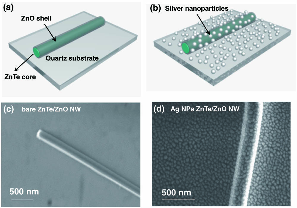
As the host nonlinear dielectric material, ZnTe has a large second-order nonlinear susceptibility of around 785 nm [3] and also a large refractive index [15], which is expected to achieve optical field confinement in ZnTe NWs with a high nonlinear conversion efficiency. In this work, the choice of 785 nm was preferred as the FW wavelength, considering that the highest power output of the employed Ti:sapphire pulsed laser is available at 785 nm and the photon energy is less than the bandgap energy of ZnTe (2.26 eV). As schematically illustrated in Fig. 1(a), with careful control of the oxidization process, ZnTe NWs were conformally surrounded by a thin ZnO shell layer, which is beneficial for concentrating more light into the ZnTe NW core and thus enhancing the nonlinear process [16]. Moreover, the ZnO shell has an additional benefit to the SHG process due to its comparably high second-order nonlinear susceptibility (10.2 pm/V at 800 nm [17]). The Ag-NP-decorated ZnTe/ZnO core–shell NW structure [see Fig. 1(b)] is expected to serve as scattering centers to enhance the forward light scattering into NWs once the photon energy of incident light matches the LSPR’s energy of the metal NPs, thus enhancing the light trapping from leaking out [18].
Sign up for Photonics Research TOC. Get the latest issue of Photonics Research delivered right to you!Sign up now
Figure 1.ZnTe/ZnO core–shell NWs. (a), (b) 3D schematic illustrations and (c), (d) top-view SEM images of a bare and Ag-NP-decorated ZnTe/ZnO core–shell NW on quartz substrate, respectively.
For NW growth, a 3-nm-thick Au layer was deposited on a GaSb (100) wafer by using an electron beam evaporation system (PVD75, Kurt J. Lesker Company) after removing the native oxide using dilute hydrofluoric (HF) acid. The wafer was annealed in Ar ambient at 380°C for 10 min to produce Au NPs as the growth catalysts. ZnTe NWs were then grown via the vapor–liquid–solid (VLS) growth mechanism at a substrate temperature of 470°C in a horizontal quartz tube furnace by using a homemade chemical vapor transport system. The detailed growth conditions and the quality of ZnTe NWs have been described elsewhere [19]. Subsequently, particular care was taken to control the oxidization of ZnTe NWs at 250°C. ZnTe/ZnO NWs were then transferred onto the quartz substrate, which have a uniform diameter of 220 nm and a length of over 10 μm. The conformal ZnTe/ZnO core–shell NWs were achieved with a shell thickness of 10 nm and a core diameter of around 200 nm. Finally, the Ag thin film was deposited on the ZnTe/ZnO NWs by using an electron-beam evaporation method, and rapid thermal annealing in nitrogen ambient for 30 s was subsequently performed to form the NPs.
Figure 1(c) shows the typical morphology of a ZnTe/ZnO core–shell single NW with a long length of over 10 μm, as characterized by scanning electron microscopy (SEM). The transferred ZnTe/ZnO NWs have a uniform diameter of 220 nm, which is composed of a ZnO shell thickness of 10 nm and a ZnTe core diameter of around 200 nm. The top-view SEM image in Fig. 1(d) shows that the Ag NPs have a sheet density of with an average diameter of 25 nm, which were randomly distributed on the surface of the ZnTe/ZnO core–shell structure and quartz substrate.
3. RESULTS AND DISCUSSION
A. Experimental Setup
The SHG characterization was performed at room temperature by using a Ti:sapphire femtosecond (fs) pulsed laser. The pulse width and repetition rate were 150 fs and 80 MHz, respectively. The fundamental wavelength can be tuned from 700 to 1100 nm, and the incident power ranged from 0.6 to 1.38 W for the incident wavelength of 785 nm. The focusing spot size was 2.5 μm, which ensured the excitation uniformity covering the entire NW width. Full details on the measurement setup have been described in our previous reports [20,21]. Considering the Ag reflection, both optical pumping and signal collection were performed from the backside of the quartz substrate, while the bare NW was characterized using a typical front-illumination configuration.
B. Characterization and Mechanism of Enhanced SHG from Ag-NP-Decorated NWs
Figures 2(a) and 2(b) show the power-dependent SHG far-field spectra of the bare and Ag-NP-decorated ZnTe/ZnO NW under TE or TM excitation, respectively, with respect to the referenced quartz substrate. The configuration of TE (TM) excitation is defined as the electric field of incident light perpendicular (parallel) to the NW long axis. All SHG far-field spectra exhibit prominent peaks at 392.5 nm, which represents the exactly frequency-doubling signal of the FW laser (785 nm), indicating the generation of second-order nonlinear processes. When the excitation laser was moved far away from the NWs and focused on the bare quartz or Ag NP coated regions, there was no measurable SHG signal. It is because the second-order nonlinear susceptibility of Ag is only several fm/V [22], which is three orders lower than that of ZnTe and ZnO materials. Therefore, the distinct SHG output is produced from the ZnO/ZnTe active material. Furthermore, no peaks were observed from defect-related photoluminescence or two-photon excited fluorescence, implying the high crystalline quality of ZnTe NWs used herein. Figures 2(c) and 2(d) show the power dependences of SHG intensity under both TE and TM excitations in logarithmic scale, respectively, which are well fitted by a quadratic relation, confirming the nonlinear nature of SHG processes. With respect to the bare NW, the SH output of the Ag-NP-decorated NW shows a remarkable enhancement of 7.2 and 16.6 times in magnitude at an FW power of 1.28 W under TE and TM excitations, respectively; see Figs. 2(c) and 2(d).
Figure 2.Enhanced frequency conversion from the Ag-NP-decorated ZnTe/ZnO NW plasmonic–dielectric coupler. (a), (b) Power-dependent SHG outputs of bare and Ag-NP-decorated ZnTe/ZnO NWs under TE and TM excitations, respectively; (c), (d) their respective quadratic relationships of average pumping power and SHG outputs under TE and TM excitations.
In light of SHG mechanisms, the enhancement of the SH outputs is a consequence of local field enhancements at both fundamental and SH frequencies. To get insight into the contribution of dielectric resonance to SHG enhancement, two-dimensional finite-difference time-domain (FDTD) simulations have been performed to calculate the absorption cross section () of ZnTe/ZnO NWs, assuming an infinite NW length. The spectral engineering is achievable by tuning the core diameter of ZnTe () under TE and TM incidences, as illustrated in Figs. 3(a) and 3(b). Here, the total diameter of the ZnTe/ZnO core–shell NW () equals , and is the ZnO shell thickness. The marked peaks correspond to the specific TE and TM resonance modes, which were verified to have strong light confinement capability within NWs [23]. For a long cylindrical ZnTe/ZnO NW, dielectric resonance modes, e.g., , , and , are approximately degenerate [23,24].
Figure 3.Dielectric resonances and LSPR supported in Ag-NP-decorated ZnTe/ZnO NWs. (a), (b) Calculated absorption cross section () of a bare ZnTe/ZnO NW on quartz under TE and TM excitations, respectively. The corresponding absorption spectra of a bare NW () and the relevant dielectric resonance modes are shown in the top plots of (a) and (b). Insets: magnetic/electric field ( or ) distribution of and modes. (c) Calculated and of the ZnTe/ZnO NW decorated by Ag NPs with an average diameter of 25 nm. Insets: calculated -distribution of the LSPR modes at 420 nm under TE and TM excitations. (d) Measured transmission, reflection, and absorption spectra of Ag-decorated ZnTe/ZnO NWs.
In particular, with , the resonances of modes at 785 nm and modes near 392.5 nm simultaneously occur, both of which exactly match the FW and SH wavelengths, respectively. The of the bare NW with are highlighted for both polarization cases in the top plots of Figs. 3(a) and 3(b), and the inset figures show their magnetic/electric field distributions of low-order dielectric resonance modes ( and ). The observed “hot spots” indicate the strong confinement of electromagnetic field within NW, which are expected to enhance the SHG performance. Especially, owing to the sub-wavelength diameter, the field configuration of exhibits a typical leaky-mode resonance, which interacts more effectively with the outside media and functions as an efficient optical nanoantenna [23]. Simultaneously, high-order modes ( and ) near 392.5 nm are beneficial for the strong confinement of SH waves with an expected local field enhancement. Therefore, the dual-wavelength matching of distinct dielectric resonances at both FW and SH wavelengths is essential for achieving SHG enhancement.
Despite the promising dielectric resonance, the SHG output from the bare NW is still far from expected as compared to that decorated with Ag NPs, which results from the absence of LSPR modes at the SH frequency. Inferred from the electrostatics approximations [25], the Ag NPs dispersed on the NW surface well support the plasmonic-coupling resonances in a wide spectral range, and the resonance behavior is sensitive to the dimensions of metal NPs and the material of the surrounding media. Considering the contribution of electric dipoles, the cross sections of scattering () and absorption () for a metal particle with a diameter of are given by [25] where and are the dielectric functions of the metal NPs and surrounding medium, respectively. Figure 3(c) shows the calculated wavelength dependence of and for Ag NPs with . The absorption and scattering peaks for Ag NPs on quartz are dominant at 365 nm, and are redshifted to 380 nm and 440 nm for the cases of Ag NPs on ZnO and ZnTe surfaces, respectively. Therefore, it is safe to say that the maximum of and lies between 380 nm and 440 nm for the Ag-NP-decorated ZnTe/ZnO core–shell NW. To understand the plasmonic coupling behavior, we performed FDTD simulations of the spatial distribution of the near-field amplitude for the Ag NP coupled NW. As illustrated in the inset of Fig. 3(c), the plasmonic coupling through LSPRs leads to the strong field distribution, extending into the ZnO/ZnTe NW at the SH frequency. To verify the occurrence of LSPR modes, the transmission, reflection, and absorption spectra of the Ag-decorated ZnO/ZnTe NWs have been characterized. As the distribution density of the transferred NWs is quite low on quartz, the results shown in Fig. 3(d) reflect mainly the optical properties of the Ag NPs randomly distributed on quartz substrate. The absorption peak and reflection dips at 360 nm show excellent consistence with the scattering/absorption cross-section peaks at 365 nm in Fig. 3(c), which is a fingerprint of the excitation of LSPRs. As a consequence, the plasmonic coupling between Ag NPs and ZnTe/ZnO NWs is expected to result in the additional local field enhancement at the SH frequency, which accounts for the improved frequency upconversion efficiency with respect to the bare NW [26]. The mechanisms of SHG enhancement in terms of LSPRs can be further verified through Raman scattering characteristics of the bare and Ag-NP-decorated ZnO/ZnTe NWs. Herein, a 633 nm laser was chosen as the excitation source, which has photon energy less than the bandgap energy of ZnTe (2.25 eV). Thus, together with the absence of defect-related photoluminescence, the Raman scattering could be regarded as a non-resonant configuration. Indeed, as shown in Fig. 4(a), for the bare ZnTe/ZnO core–shell NW, non-resonance Raman scattering consequently occurs with a rather low vibrational intensity of longitudinal-optical (LO) phonon modes, whereby the scattering cross section is extremely small. In comparison, for the Ag-NP-decorated NW, distinct enhancement of Raman scattering was observed, as shown in Fig. 4(b). Especially, the 1LO phonon mode was enhanced by at least one order in magnitude with respect to the bare NW. In the electromagnetic mechanism, plasmonic metal NPs are favorable to significantly enhance local electric fields at the metal–dielectric interface, which in turn leads to more intense electronic transitions in the near surface of ZnTe/ZnO NW. It is widely reported as surface-enhanced Raman scattering (SERS), whereby Raman scattering intensity scales roughly with [27,28]. Furthermore, it has been proposed that multiple Rayleigh scatterings between the Raman objective and metallic nanostructures will notably modify the localized electromagnetic field, so that the Raman activation and radiation processes would be dramatically enhanced simultaneously. For clarity, the dependence of integrated 1LO phonon intensity () on the excitation energy () is summarized in logarithmic scale in Fig. 4(c), which is well described by the power law of . The fittings give rise to the power exponent of 0.45 and 0.58 for the bare and Ag-decorated NWs, respectively, indicative of enhanced light–matter interaction. Note that the essentials of the observed SERS and enhanced SHG share the same mechanism of macroscopic local field enhancement [29]. It means that the appropriate engineering of Ag NPs’ dimensions offers the possibility to manipulate LSPRs with strong local-field confinements, which is expected to contribute to the simultaneous enhancement of the SHG output and SERS.
Figure 4.Enhanced Raman scattering from the plasmonic–dielectric NW coupler. (a), (b) Raman scattering spectra measured from a bare and an Ag-NP-decorated ZnO/ZnTe NW with various excitation powers, respectively. (c) Raman scattering intensity of the 1LO phonon mode as a function of excitation power for a bare and an Ag-NP-decorated ZnO/ZnTe NW. All intensities of Raman scattering are with respect to the referenced quartz substrate.
C. Excitation Polarization and Wavelength Dependence of SHG Signals
Besides the enhanced nonlinear optical conversion efficiency, highly polarized SHG output is also desirable for developing the coherent light source. Figure 5(a) shows the polarization response of SHG signals from the Ag-NP-decorated ZnTe/ZnO NWs. The measurement configuration is similar to that used in Fig. 2, and a polarizer is mounted in front of the spectrometer to control the polarization of SHG signals. Similar to the definition of TE(I) or TM(I) for the incident FW mode, the emitted SHG outputs with polarization perpendicular and parallel to the NW long axis are defined as TE(O) and TM(O) configurations, respectively. Upon excitation with transverse polarized light [TE(I)], both SHG outputs across and along the NW axis are relatively weak and almost polarization independent, while the intensity enhancement and polarization anisotropy of SHG intensity [TM(O) and TE(O)] are simultaneously achieved when excited in the longitudinally polarized light [TM(I)] configuration. It is understood that in high-aspect-ratio NWs, a high anisotropic polarization response for guided modes is expected. The longitudinal polarization is always more efficient than the transverse polarization in establishing the internal electromagnetic field, and the smaller the NW diameter, the larger the anisotropy in the absorption behavior, as evidenced in Fig. 2 [30]. These results agree well with the following FW electrical-field () polarization dependence [31]: where is the angle between the NW long axis and the electric field of the incident FW, is the second-order susceptibility, and is the intensity of the FW (SH) wave. In the case of or 270°, i.e., TE(I) excitation, the plasmonic coupling is weak, which has a small influence on the NW response for both longitudinal and transverse polarizations. In comparison, under TM(I) excitation with or 180°, the electromagnetic field of the in-coming FW waves is concentrated into the nonlinear region due to the strong plasmonic coupling, which alters significantly the polarization sensitive optical behavior together with the directional SHG outputs [32].
Figure 5.Polarization controllability and broadband output of the SHG. (a) Polarized SHG signals from an Ag-NP-decorated ZnTe/ZnO NW excited under FW wavelength of 785 nm under TE and TM configurations. (b) SHG spectra measured at different pump wavelengths, and the wavelength-dependent FW pumping power is shown for reference.
Broadband nonlinear optical conversion has also been expected in semiconductor nanostructures owing to the less stringent phase-matching conditions. Figure 5(b) shows the broadband enhanced SHG processing in the Ag-NP-decorated ZnTe/ZnO NW with the incident FW ranging from 740 to 1040 nm. For calibration, the pumping power as a function of FW wavelength is also shown by open circles. Overall, the broadband SHG signals were generated over a broad spectral range from the single NW with a large surface-to-volume ratio. This large ratio is expected to break the structural symmetry of the surface area and induces dipoles oscillating with the electromagnetic field, which enhances the surface second-order nonlinearity without signal propagation. Combined with Ag plasmonic nanostructures, the SHG outputs exhibit distinct wavelength anisotropy with an intense peak around 420 nm and a distinct valley around 380 nm. The wavelength corresponding to the maximum SHG output is in excellent agreement with the guided modes and also consistent with the LSPR modes at the interface of Ag NPs and ZnTe/ZnO NW, as shown in Fig. 3(c). For the drop of SHG output around 380 nm, it could result from the band-to-band self-absorption of the ZnO shell that has a bandgap energy of 3.26 eV at room temperature [33].
4. CONCLUSION
In summary, we have demonstrated a highly enhanced and polarized SHG output in a hybrid structure that consists of Ag plasmonic NPs and a ZnTe/ZnO single NW. With careful design and precisely controlled dimensions of metal–dielectric hybrid nanostructures, the SHG signal exhibits significant enhancement and excellent polarization controllability with respect to the bare NW. Theoretical calculations indicate that the simultaneous occurrence of dielectric resonances and metal NP induced LSPRs is responsible for the enhanced electromagnetic field intensity and efficient frequency upconversion, as evidenced by the enhanced absorption and SERS. Tailoring the light–matter interaction in such a hybrid nonlinear medium provides an alternative and efficient strategy to enhance the nonlinear process, which holds great promise for assembling high-performance nanophotonic devices towards applications of all-optical signal processing and short-wavelength laser sources.