• Photonics Research
  • Vol. 7, Issue 6, 687 (2019)
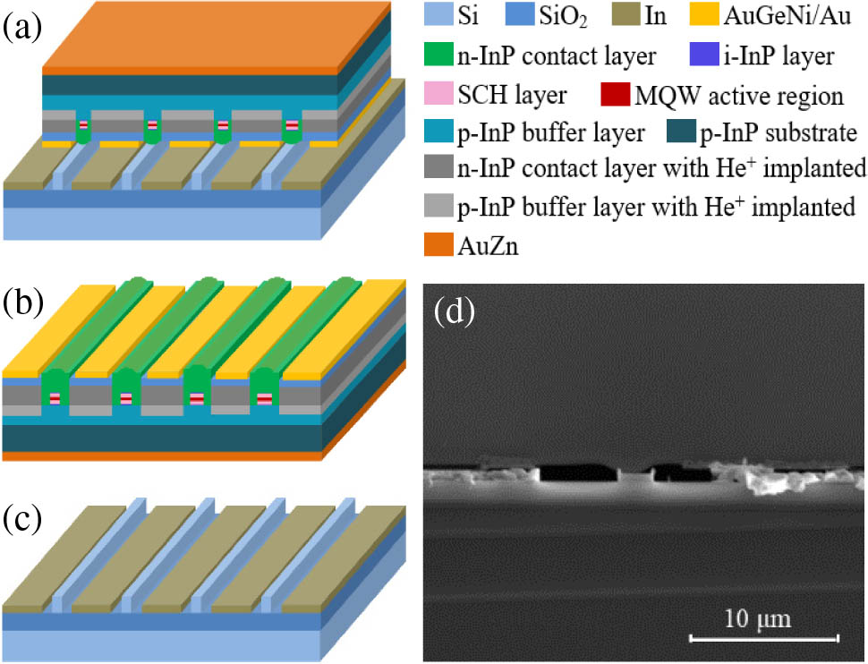
Yajie Li1、2、3, Hongyan Yu1、2、3、4, Wengyu Yang1、2、3, Chaoyang Ge5, Pengfei Wang1、2、3, Fangyuan Meng1、2、3, Guangzhen Luo1、2、3, Mengqi Wang1、3, Xuliang Zhou1、3, Dan Lu1、2、3, Guangzhao Ran5, and Jiaoqing Pan1、2、3、6
Author Affiliations
  • 1Key Laboratory of Semiconductor Materials Science, Institute of Semiconductors, Chinese Academy of Sciences, Beijing 100083, China
  • 2Center of Materials Science and Optoelectronics Engineering, University of Chinese Academy of Sciences, Beijing 100049, China
  • 3Beijing Key Laboratory of Low Dimensional Semiconductor Materials and Devices, Beijing 100083, China
  • 4e-mail: hyyu09@semi.ac.cn
  • 5State Key Laboratory for Artificial Microstructure and Mesoscopic Physics, School of Physics, Peking University, Beijing 100871, China
  • 6e-mail: jqpan@semi.ac.cn
  • show less
    DOI: 10.1364/PRJ.7.000687 Cite this Article Set citation alerts
    Yajie Li, Hongyan Yu, Wengyu Yang, Chaoyang Ge, Pengfei Wang, Fangyuan Meng, Guangzhen Luo, Mengqi Wang, Xuliang Zhou, Dan Lu, Guangzhao Ran, Jiaoqing Pan. 4λ hybrid InG[J]. Photonics Research, 2019, 7(6): 687 Copy Citation Text show less
    (a) Schematic diagram of the 4–λ hybrid InGaAsP-Si evanescent laser array (not to scale). (b) Schematic diagram of the InGaAsP/InP MQW DFB laser array (not to scale). (c) Schematic diagram of the SOI substrate with Si waveguides (not to scale). (d) SEM image after selective area metal bonding the InGaAsP/InP MQW DFB laser array to the SOI substrate.
    Fig. 1. (a) Schematic diagram of the 4λ hybrid InGaAsP-Si evanescent laser array (not to scale). (b) Schematic diagram of the InGaAsP/InP MQW DFB laser array (not to scale). (c) Schematic diagram of the SOI substrate with Si waveguides (not to scale). (d) SEM image after selective area metal bonding the InGaAsP/InP MQW DFB laser array to the SOI substrate.
    (a) Effective index and lasing wavelength varying with the III–V ridge waveguide width. (b), (c) Calculated optical field distributions of the hybrid laser with a 2.2-μm-wide III–V ridge waveguide when the alignment errors are 0 μm and 0.5 μm, respectively. (d), (e) Calculated optical field distributions of the hybrid laser with a 2.6-μm-wide III–V ridge waveguide when the alignment errors are 0 μm and 0.5 μm, respectively.
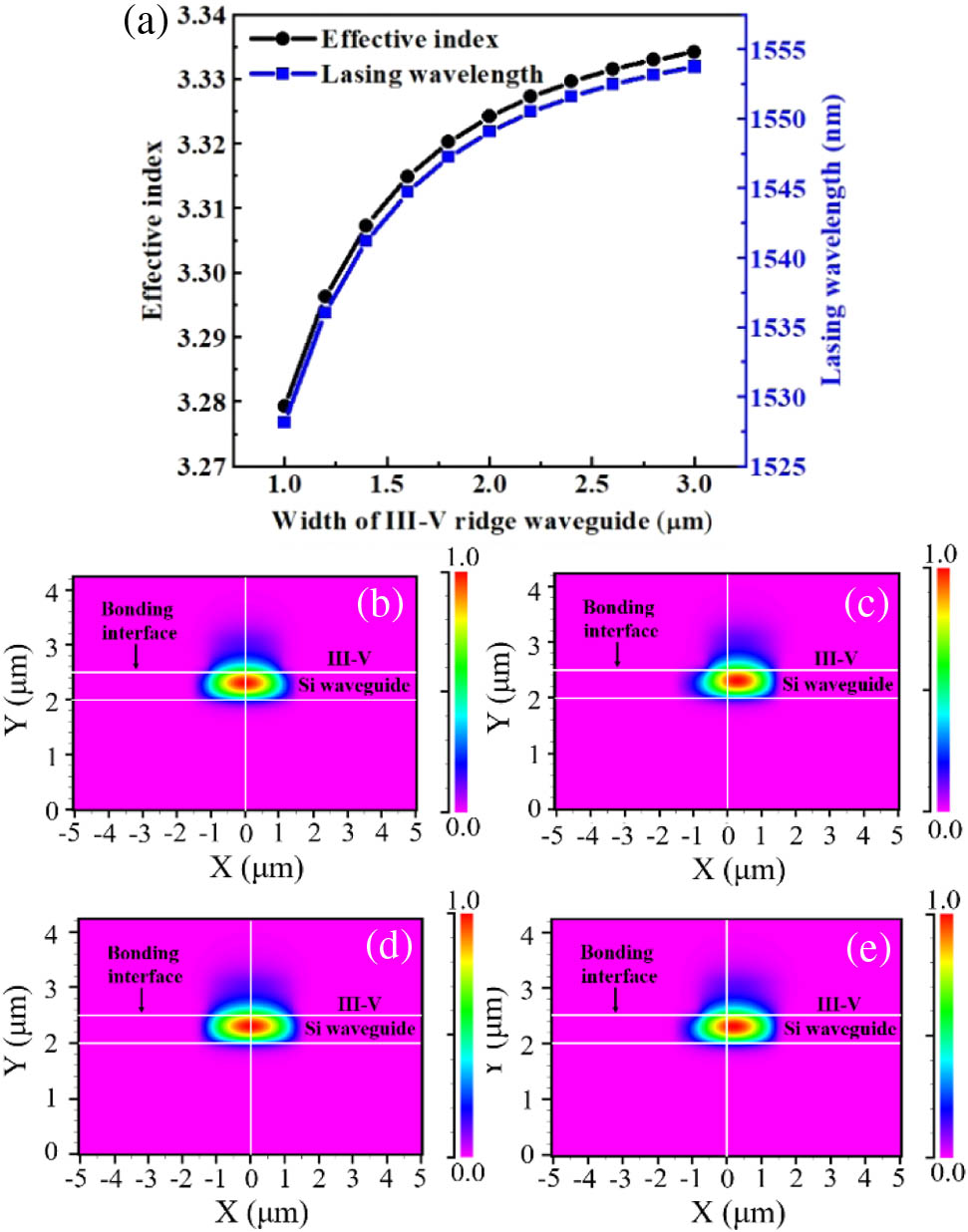
    Fig. 2. (a) Effective index and lasing wavelength varying with the III–V ridge waveguide width. (b), (c) Calculated optical field distributions of the hybrid laser with a 2.2-μm-wide III–V ridge waveguide when the alignment errors are 0 μm and 0.5 μm, respectively. (d), (e) Calculated optical field distributions of the hybrid laser with a 2.6-μm-wide III–V ridge waveguide when the alignment errors are 0 μm and 0.5 μm, respectively.
    (a) P−I (solid lines) and V−I (dotted lines) curves of the 4–λ hybrid InGaAsP-Si evanescent laser array measured under CW operation at 25°C. (b) Natural log of Ith as a function of the operating temperature for the 4–λ hybrid InGaAsP-Si evanescent laser array.
    Fig. 3. (a) PI (solid lines) and VI (dotted lines) curves of the 4λ hybrid InGaAsP-Si evanescent laser array measured under CW operation at 25°C. (b) Natural log of Ith as a function of the operating temperature for the 4λ hybrid InGaAsP-Si evanescent laser array.
    Tests were carried out under CW operation of 20 mA at 25°C. (a) Spectral characteristics of the 4–λ hybrid InGaAsP-Si evanescent laser array. Inset is the lasing spectra over a 100 nm span. (b) SMSRs of the lasing wavelengths before and after bonding.
    Fig. 4. Tests were carried out under CW operation of 20 mA at 25°C. (a) Spectral characteristics of the 4λ hybrid InGaAsP-Si evanescent laser array. Inset is the lasing spectra over a 100 nm span. (b) SMSRs of the lasing wavelengths before and after bonding.
    SMSRs of the 4–λ hybrid InGaAsP-Si evanescent laser array measured under CW operation. (a) SMSR versus the injection current, measured at 25°C. (b) SMSR versus the operating temperature, measured at 20 mA.
    Fig. 5. SMSRs of the 4λ hybrid InGaAsP-Si evanescent laser array measured under CW operation. (a) SMSR versus the injection current, measured at 25°C. (b) SMSR versus the operating temperature, measured at 20 mA.
    Layer NameCompositionDoping ConcentrationThickness
    n-InP layerInP>5×10¹⁹  cm3500 nm
    i-InP layerInPUndoped5 nm
    Upper SCH layerInGaAsP, 1.2QaUndoped80 nm
    MQWInGaAsP, 1.59QUndoped4  nm×6
    InGaAsP, 1.15QUndoped9  nm×5
    Lower SCH layerInGaAsP, 1.2QaUndoped80 nm
    i-InP layerInPUndoped26 nm
    p buffer layerInP1–5×10¹⁷  cm3670 nm
    Table 1. Epitaxial Structure of the InGaAsP/InP MQW DFB Laser
    Yajie Li, Hongyan Yu, Wengyu Yang, Chaoyang Ge, Pengfei Wang, Fangyuan Meng, Guangzhen Luo, Mengqi Wang, Xuliang Zhou, Dan Lu, Guangzhao Ran, Jiaoqing Pan. 4λ hybrid InG[J]. Photonics Research, 2019, 7(6): 687
    Download Citation