Abstract
A hybrid InGaAsP-Si evanescent laser array is obtained by bonding III–V distributed feedback lasers to a silicon on insulator (SOI) substrate using a selective area metal bonding technique. Multiple wavelengths are realized by varying the width of the III–V ridge waveguide. The threshold current is less than 10?mA for all wavelength channels under continuous-wave (CW) operation at room temperature, and the lowest threshold current density is . The side mode suppression ratio (SMSR) is higher than 40?dB for all wavelength channels when the injection current is between 20?mA and 70?mA at room temperature, and the highest SMSR is up to 51?dB. A characteristic temperature of 51?K and thermal impedance of 144°C/W are achieved on average. The hybrid InGaAsP-Si evanescent laser array exhibits a low threshold and high SMSR under CW operation at room temperature. The low power consumption of this device makes it very attractive for on-chip optical interconnects.1. INTRODUCTION
In recent years, silicon photonic integrated circuits (PICs) have been extensively studied and developed, and are becoming a promising platform for higher-speed interconnects and complex higher functionality with low cost [1,2]. However, silicon is an indirect bandgap semiconductor, which is extremely hard for efficient lasing. The III–V materials with direct bandgap can be used along with the silicon to realize on-chip lasing on the silicon substrate. Wafer bonding is an effective solution to address these challenges [3–6], which can easily integrate III–V materials and Si through a simple fabrication process and overcome the differences in the natural properties of the materials. Several bonding methods have been reported, typical of which include direct wafer bonding [7], benzocyclobutene (BCB) bonding [8], and metal bonding [9].
The silicon on insulator (SOI) substrate is generally selected for bonding with III–V materials, since the buried oxide layer can prevent the light in the Si waveguide from leaking into the silicon substrate [10], and many building blocks for PICs have been demonstrated on SOI substrates [11–15]. The power consumption of the data centers already represents several percent of the global electricity consumption, and the percentage is expected to rise; thus, it is essential that the signal sources such as semiconductor lasers used in the optical interconnects have very low power consumption [16,17]. In silicon-based on-chip optical interconnection, there is a strong need for low-power-consumption silicon-based laser sources that are capable of generating laser from Si waveguides [18]. Bowers’ group demonstrated the first electrically pumped distributed feedback (DFB) silicon evanescent laser [19], with maximum output power of 5.4 mW and threshold current density of at 10°C. Keyvaninia et al. reported a heterogeneously integrated III–V-on-silicon second-order DFB laser using BCB bonding [8], with a high side mode suppression ratio (SMSR) of 50 dB at 100 mA and threshold current density of at 20°C. We integrated a buried ridge stripe (BRS) structure of the III–V gain materials with the Si waveguide by a selective area metal bonding (SAMB) method, with a threshold current density of at room temperature [20]. For the BRS structure, the multi-quantum-well (MQW) active region is surrounded by the n-InP, which has the advantages of a low threshold, high thermal performance, good optical field, and carrier confinement. The SAMB method can effectively avoid the metal absorption of the light by laterally separating the optical coupling region from the metal bonding region [21–23].
In this paper, we demonstrate a hybrid InGaAsP-Si evanescent laser array, which is obtained by bonding a III–V DFB laser array to an SOI substrate using the SAMB technique. The III–V DFB lasers employ BRS structure to provide optical gain. The Si waveguides are used for optical transmission. The multiple wavelengths are realized by varying the width of the III–V ridge waveguide. The threshold current is less than 10 mA for all wavelength channels under continuous-wave (CW) operation at room temperature, and the lowest threshold current density is . The SMSR is higher than 40 dB for all wavelength channels when the injection current is between 20 mA and 70 mA at room temperature, and the highest SMSR is up to 51 dB. A characteristic temperature of 51 K and thermal impedance of 144°C/W are achieved on average. Compared with our previous work on the hybrid InGaAsP-Si evanescent laser array [24], the threshold current, output power, and SMSR reported in this work have been improved dramatically, which may provide an attractive solution for on-chip optical interconnects.
Sign up for Photonics Research TOC. Get the latest issue of Photonics Research delivered right to you!Sign up now
2. DEVICE DESIGN AND FABRICATION
The hybrid InGaAsP-Si evanescent laser array was fabricated by integrating an InGaAsP/InP MQW DFB laser array with an SOI wafer having 3-μm-wide Si waveguides, using the SAMB method, as shown in Fig. 1(a). The InGaAsP/InP MQW DFB laser was grown on a p-InP substrate by metal organic chemical vapor deposition (MOCVD) using two growth steps, and the specific epitaxial structure is shown in Table 1. In the first epitaxy, a 670-nm-thick p-InP buffer layer, a 26-nm-thick undoped InP layer, and an 80-nm-thick lower separate confinement heterostructure (SCH) layer were grown on the p-InP substrate, followed by an MQW active region, an 80-nm-thick upper SCH layer, and a 5-nm-thick undoped InP layer. After the first epitaxy, 55-nm-deep first-order gratings were prepared into the upper SCH layer by conventional holographic exposure and reactive ion etching (RIE) dry etch. The grating period () was 233 nm, and the duty cycle was 50%. Then, III–V ridge waveguides of different widths were defined by photolithography and wet chemical etching with bromine solution. Thereafter, a second epitaxy was performed to grow a 500-nm-thick n-InP layer for providing better optical confinement and serving as a contact layer for the cathode. After that, was implanted down to the p-InP layer by using the photoresist as a masking layer to form highly resistive regions on both sides of the BRS. A 300-nm-thick layer was deposited on the n-InP layer with a 20-μm-wide window opened on top of the BRS to further improve the lateral current confinement. AuGeNi/Au was deposited onto the n-InP layer with 10-μm-wide optical coupling windows opened right above the III–V ridge stripe, playing the roles of cathode and bonding metal. AuZn was thermally evaporated onto the p-side after thinning and polishing the InP substrate. Last, the wafer was cleaved to a laser array with a cavity length of 300 μm, as shown in Fig. 1(b), waiting to be bonded on the SOI wafer.
| Layer Name | Composition | Doping Concentration | Thickness |
| n-InP layer | InP | >5×1019 cm−3 | 500 nm |
| i-InP layer | InP | Undoped | 5 nm |
| Upper SCH layer | InGaAsP, 1.2Qa | Undoped | 80 nm |
| MQW | InGaAsP, 1.59Q | Undoped | 4 nm×6 |
| InGaAsP, 1.15Q | Undoped | 9 nm×5 |
| Lower SCH layer | InGaAsP, 1.2Qa | Undoped | 80 nm |
| i-InP layer | InP | Undoped | 26 nm |
| p buffer layer | InP | 1–5×1017 cm−3 | 670 nm |
Table 1. Epitaxial Structure of the InGaAsP/InP MQW DFB Laser
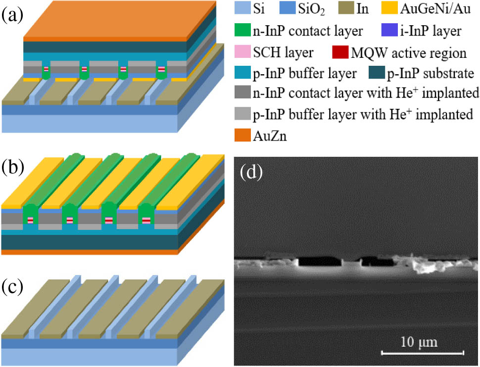
Figure 1.(a) Schematic diagram of the hybrid InGaAsP-Si evanescent laser array (not to scale). (b) Schematic diagram of the InGaAsP/InP MQW DFB laser array (not to scale). (c) Schematic diagram of the SOI substrate with Si waveguides (not to scale). (d) SEM image after selective area metal bonding the InGaAsP/InP MQW DFB laser array to the SOI substrate.
The DFB grating period on the III–V ridge waveguide is a fixed value (). The multi-wavelength operation of the laser array is achieved by varying the width of the III–V ridge waveguide. The effective index () is a function of the ridge waveguide width, as shown in Fig. 2(a). It can be seen that when the waveguide width increases from 1.0 μm to 3.0 μm, the increases from 3.28 to 3.33, and the lasing wavelength increases from 1528 nm to 1553 nm (estimated by ). We chose the widths of the III–V ridge waveguides to be 2.2 μm, 2.3 μm, 2.4 μm, and 2.6 μm, respectively.

Figure 2.(a) Effective index and lasing wavelength varying with the III–V ridge waveguide width. (b), (c) Calculated optical field distributions of the hybrid laser with a 2.2-μm-wide III–V ridge waveguide when the alignment errors are 0 μm and 0.5 μm, respectively. (d), (e) Calculated optical field distributions of the hybrid laser with a 2.6-μm-wide III–V ridge waveguide when the alignment errors are 0 μm and 0.5 μm, respectively.
On the SOI substrate, 3-μm-wide and 500-nm-high Si waveguides were fabricated by photolithography and inductively coupled plasma (ICP) etching, as shown in Fig. 1(c). The bonding metal indium (In) was prepared in the selected regions on the SOI substrate by a lift-off process, which was about 6 μm away from the Si waveguides on each side. The InGaAsP/InP MQW DFB laser array with a cavity length of 300 μm was flip-chip bonded to the SOI substrate by using the SAMB method, as shown in Fig. 1(d). The alignment accuracy of the Finetech Lamda A6 bonder is . The bonding process lasted for 5 min at a temperature of 200°C, under pressure of about 23 MPa. The III–V DFB lasers employ BRS structure to provide optical gain. The Si waveguides are used for optical transmission. For performance testing, a negative electrode pad was formed on the In metal, and the positive electrode pad was formed on the AuZn metal. The electrons were injected from the In cathode and traveled transversely in the AuGeNi/Au and n-InP layers, then flowed into the III–V MQW active region. The holes were injected from the top AuZn anode, combined with the electrons in the III–V MQW active region. Through simulation, we found that when a III–V ridge waveguide with a width of 2.2–2.6 μm was aligned with a 3-μm-wide Si waveguide, the hybrid laser could operate in a fundamental transverse mode state, as shown in Figs. 2(b) and 2(d), and most of the light was evanescently coupled to the Si waveguide. If the alignment error was , there was still an optical fundamental transverse mode in the hybrid laser, as shown in Figs. 2(c) and 2(e). The calculated optical field was still mainly in the Si waveguide, but the mode center deviated from the geometrical center of the Si waveguide, as indicated by the vertical white line.
3. EXPERIMENTAL RESULTS AND DISCUSSION
The hybrid InGaAsP-Si evanescent lasers were operated under CW operation at room temperature. The maximum optical output powers () from a single facet were 0.83 mW, 1.19 mW, 2.52 mW, and 3.01 mW, respectively, as shown in Fig. 3(a), and the threshold currents () were 9.66 mA, 5.07 mA, 4.35 mA, and 7.88 mA, respectively. The III–V ridge waveguide width value obtained in the experiment was about 0.5 μm smaller than the design value on the lithographic plate, owing to the side etching caused by the wet etching. Therefore, the threshold current densities () of the hybrid lasers were , , , and , respectively. The differences in the threshold, output power, and external quantum efficiency among 4-channel lasers are caused mainly by the following factors: uniformity of the epitaxial material, uniformity of the device fabrication process, and the difference in the III–V waveguide width. The changes in the threshold current, maximum output power, and external quantum efficiency before and after bonding were, respectively, as follows: , , . The above comparisons were performed using the average of the 4-channel lasers, and the 4-channel lasers before and after the bonding are distinguished by subscripts 1 and 2, respectively. After bonding, the threshold current increased, and the maximum output power and external quantum efficiency decreased, caused mainly by an increase in the internal loss and reduction in the confinement factor of the active region. The optical field before bonding is distributed mostly in the III–V active region. After bonding, the optical field is coupled into the Si waveguide through the n-InP contact layer. Therefore, the increase in light absorption by the n-InP contact layer is one of the main reasons for the increase in internal loss. When the light is evanescently coupled from the BRS waveguide to the Si waveguide, a small amount of light leaks into the air, especially if the two waveguides are not aligned or not in close contact, which results in an increase in the internal loss of the hybrid laser. The sidewall of the Si waveguide prepared by ICP etching causes some loss of light, thereby increasing the internal loss of the hybrid laser.
Figure 3.(a) (solid lines) and (dotted lines) curves of the hybrid InGaAsP-Si evanescent laser array measured under CW operation at 25°C. (b) Natural log of as a function of the operating temperature for the hybrid InGaAsP-Si evanescent laser array.
The threshold current is a function of the operating temperature, and it can generally be described by the following empirical formula [25]: where is the operating temperature, is known as the characteristic temperature, and both temperatures are given in degrees Kelvin K. can be extracted by fitting the natural logarithm of versus the operating temperature. As shown in Fig. 3(b), the reciprocal of the slope is . The characteristic temperature of the hybrid evanescent laser array is 51 K on average, which falls within the range of typical characteristic temperatures for heterogeneous laser sources [10]. The characteristic temperature of our previously fabricated InGaAsP/Si hybrid single-mode laser is 36 K [23]. The increase in the characteristic temperature is due mainly to the improvement in the fabrication process of the p-electrode. However, the resistance is still relatively large, as shown in the curves in Fig. 3(a), so it is necessary to continue to optimize the electrode process or the doping concentration of the III–V contact layer.
The lasing spectra of the hybrid evanescent lasers were measured by the Yokogawa AQ6370C optical spectrum analyzer with a spectral resolution of 0.1 nm under the injection current of 20 mA at 25°C, as shown in Fig. 4(a). The center wavelengths were 1537.2 nm, 1538.8 nm, 1541.0 nm, and 1544.2 nm, respectively. The center wavelengths were almost the same before and after bonding. For each wavelength channel, the mode spacing before and after bonding was almost the same, both about 1.052 nm. The wavelength separations between two adjacent channels were 1.6 nm, 2.2 nm, and 3.2 nm, respectively. A narrower wavelength separation between the two adjacent channels can be achieved by reducing the spacing of the III–V ridge waveguide widths. It is necessary to vary the III–V ridge waveguide width non-linearly in order to obtain a fixed wavelength spacing, due to the fact that the effective refractive index is not linearly varied with III–V ridge waveguide width. The wavelengths of the hybrid evanescent lasers measured by the experiment are not exactly the same as the calculated wavelengths, because of fabrication and calculation errors. The III–V ridge waveguide can be fabricated by ICP dry etching to realize a more precise control of the waveguide width. When the injection current was 20 mA at a temperature of 25°C, the SMSRs of the hybrid evanescent lasers before bonding were 42.9 dB, 41.0 dB, 39.2 dB, and 37.1 dB, respectively. The SMSRs after bonding were improved, as shown in Fig. 4(b), which were 48.4 dB, 45.2 dB, 44.4 dB, and 41.6 dB, respectively. It can be seen from the inset in Fig. 4(a) that the hybrid lasers operated single mode over a 100 nm span. The spectral tests before and after bonding were performed using the same optical spectrum analyzer under the same test conditions. The SMSR after bonding was 4.85 dB on average higher than that before bonding. We previously demonstrated a InGaAsP-Si DFB evanescent laser array by varying the Si waveguide width and fabricating DFB gratings on the Si waveguide [24], where the performance parameters of the device were , at 300 mA pulse current, and . For the hybrid lasers in this paper, the DFB gratings were etched in the upper SCH layer, which can avoid the air gaps caused by the gratings at the bonding interface and reduce the optical loss caused by the grating etching process on the Si waveguide.
Figure 4.Tests were carried out under CW operation of 20 mA at 25°C. (a) Spectral characteristics of the hybrid InGaAsP-Si evanescent laser array. Inset is the lasing spectra over a 100 nm span. (b) SMSRs of the lasing wavelengths before and after bonding.
The SMSRs of the hybrid evanescent lasers were higher than 40 dB when the injection current was between 20 mA and 70 mA at a temperature of 25°C, as shown in Fig. 5(a), and the highest SMSR was up to 51 dB. When the current was increased from 20 mA to 70 mA under 25°C, the wavelengths increased from [1537.22 nm, 1538.79 nm, 1540.97 nm, 1544.18 nm] to [1540.48 nm, 1542.21 nm, 1544.24 nm, 1547.26 nm], respectively. The average redshift speed of the wavelength with injection current was 0.065 nm/mA under the operating temperature of 25°C. The SMSRs of the hybrid evanescent lasers were higher than 40 dB under 35°C at an injection current of 20 mA, as shown in Fig. 5(b). When the injection current was 20 mA and the operating temperature increased from 10°C to 35°C, the lasing wavelengths of hybrid evanescent lasers were increased from [1535.85 nm, 1537.32 nm, 1539.65 nm, 1542.91 nm] to [1538.11 nm, 1539.62 nm, 1541.91 nm, 1545.20 nm], respectively. The average redshift speed of the wavelength with operating temperature was 0.091 nm/°C under CW operation. The thermal impedance of the laser is determined by the experimental shift in wavelength as a function of operating temperature under pulsed operation and as a function of electrical dissipated power () under CW operation [26]. The thermal impedance () can be written as Under pulsed operation (0.1 μs pulse width, 0.01% duty cycle, 80 mA injection current), the average value of was 0.090 nm/°C. The average value of was 12.976 nm/W under CW operation, i.e., the thermal impedance of the hybrid evanescent laser array was 144°C/W on average. Compared to the III–V/Si bonded lasers reported in Refs. [8,19], it can obtain an SMSR of up to 40 dB under lower power consumption. However, it can be seen from the curves in Fig. 3(a) that the power consumption can be continuously reduced by lowering the resistance of the device, which can be achieved by improving the fabrication process or the doping concentration of the III–V contact layer.
Figure 5.SMSRs of the hybrid InGaAsP-Si evanescent laser array measured under CW operation. (a) SMSR versus the injection current, measured at 25°C. (b) SMSR versus the operating temperature, measured at 20 mA.
4. CONCLUSION
A hybrid InGaAsP-Si evanescent laser array is obtained by SAMB of the III–V DFB lasers to the SOI substrate. The threshold current is less than 10 mA under CW operation at room temperature, and the lowest threshold current density is . The SMSR is higher than 40 dB when the injection current is between 20 mA and 70 mA, and the highest SMSR is up to 51 dB. A characteristic temperature of 51 K and thermal impedance of 144°C/W are achieved on average. The hybrid InGaAsP-Si evanescent laser array exhibits a low threshold and high SMSR under CW operation at room temperature. The low power consumption of this device makes it very attractive for on-chip optical interconnects.
References
[1] D. Liang, J. E. Bowers. Recent progress in lasers on silicon. Nat. Photonics, 4, 511-517(2010).
[2] M. J. R. Heck, J. F. Bauters, M. L. Davenport, J. K. Doylend, S. Jain, G. Kurczveil, S. Srinivasan, Y. Tang, J. E. Bowers. Hybrid silicon photonic integrated circuit technology. IEEE J. Sel. Top. Quantum Electron., 19, 6100117(2013).
[3] S. S. Sui, M. Y. Tang, Y. D. Yang, J. L. Xiao, Y. Du, Y. Z. Huang. Investigation of hybrid microring lasers adhesively bonded on silicon wafer. Photon. Res., 3, 289-295(2015).
[4] A. W. Fang, H. Park, J. E. Bowers, M. J. Paniccia, O. Cohen, R. Jones. Electrically pumped hybrid AlGaInAs-silicon evanescent laser. Opt. Express, 14, 9203-9210(2006).
[5] K. Tanabe, K. Watanabe, Y. Arakawa. III–V/Si hybrid photonic devices by direct fusion bonding. Sci. Rep., 2, 349(2012).
[6] Y. Li, Y. Zhang, L. Zhang, A. W. Poon. Silicon and hybrid silicon photonic devices for intra-datacenter applications: state of the art and perspectives. Photon. Res., 3, B10-B27(2015).
[7] H. Jan, H. Nico, J. T. C. M. Pulles, S. Esther, J. C. G. Vervest. Direct bonding and beyond. Appl. Opt., 46, 6793-6803(2007).
[8] S. Keyvaninia, S. Verstuyft, L. Van Landschoot, F. Lelarge, G. H. Duan, S. Messaoudene, J. M. Fedeli, T. De Vries, B. Smalbrugge, E. J. Geluk. Heterogeneously integrated III–V/silicon distributed feedback lasers. Opt. Lett., 38, 5434-5437(2013).
[9] H. Kim, S. Y. Ahn, S. Kim, G. Ryu, J. H. Kyhm, K. W. Lee, J. H. Park, W. J. Choi. InAs/GaAs quantum dot infrared photodetector on a Si substrate by means of metal wafer bonding and epitaxial lift-off. Opt. Express, 25, 17562-17570(2017).
[10] M. Buffolo, M. Pietrobon, C. De Santi, F. Samparisi, M. L. Davenport, J. E. Bowers, G. Meneghesso, E. Zanoni, M. Meneghini. Degradation mechanisms of heterogeneous III–V/silicon loop-mirror laser diodes for photonic integrated circuits. Microelectron. Reliab., 88–90, 855-858(2018).
[11] B. B. Bakir, A. V. D. Gyves, R. Orobtchouk, P. Lyan, C. Porzier, A. Roman, J. M. Fedeli. Low-Loss (< 1 dB) and polarization-insensitive edge fiber couplers fabricated on 200-mm silicon-on-insulator wafers. IEEE Photon. Technol. Lett., 22, 739-741(2010).
[12] M. S. Dahlem, C. W. Holzwarth, K. Anatol, F. X. Kärtner, H. I. Smith, E. P. Ippen. Reconfigurable multi-channel second-order silicon microring-resonator filterbanks for on-chip WDM systems. Opt. Express, 19, 306-316(2011).
[13] L. Virot, P. Crozat, J. M. Fédéli, J. M. Hartmann, D. Marrismorini, E. Cassan, F. Boeuf, L. Vivien. Germanium avalanche receiver for low power interconnects. Nat. Commun., 5, 4957(2014).
[14] T. Ferrotti, A. Chantre, B. Blampey, H. Duprez, F. Milesi, A. Myko, C. Sciancalepore, K. Hassan, J. Harduin, C. Baudot. Power-efficient carrier-depletion SOI Mach-Zehnder modulators for 4 × 25 Gbit/s operation in the O-band. Proc. SPIE, 9367, 93670D(2015).
[15] C. Sciancalepore, L. J. Richard, J. A. Dallery, S. Pauliac, K. Hassan, J. Harduin, H. Duprez, U. Weidenmueller, D. F. G. Gallagher, S. Menezo. Low-crosstalk fabrication-insensitive echelle grating demultiplexers on silicon-on-insulator. IEEE Photon. Technol. Lett., 27, 494-497(2015).
[16] A. Abbasi, S. Keyvaninia, J. Verbist, X. Yin, J. Bauwelinck, F. Lelarge, G. Duan, G. Roelkens, G. Morthier. 43 Gb/s NRZ-OOK direct modulation of a heterogeneously integrated InP/Si DFB laser. J. Lightwave Technol., 35, 1235-1240(2017).
[17] N. Horiuchi, S. Matsuo. A big leap in energy-saving lasers. Nat. Photonics, 7, 576(2013).
[18] D. A. B. Miller. Device requirements for optical interconnects to silicon chips. Proc. IEEE, 97, 1166-1185(2009).
[19] A. W. Fang, L. Erica, K. Ying-Hao, L. Di, J. E. Bowers. A distributed feedback silicon evanescent laser. Opt. Express, 16, 4413-4419(2008).
[20] H. Yu, L. Yuan, L. Tao, W. Chen, Y. Li, Y. Ding, G. Ran, J. Pan, W. Wang. 1550 nm evanescent hybrid InGaAsP-Si laser with buried ridge stripe structure. IEEE Photon. Technol. Lett., 28, 1146-1149(2016).
[21] L. Yuan, L. Tao, H. Yu, W. Chen, D. Lu, Y. Li, G. Ran, J. Pan. Hybrid InGaAsP-Si evanescent laser by selective-area metal-bonding method. IEEE Photon. Technol. Lett., 25, 1180-1183(2013).
[22] T. Hong, G. Z. Ran, T. Chen, J. Q. Pan, W. X. Chen, Y. Wang, Y. B. Cheng, S. Liang, L. J. Zhao, L. Q. Yin. A selective-area metal bonding InGaAsP-Si laser. IEEE Photon. Technol. Lett., 22, 1141-1143(2010).
[23] L. Yuan, L. Tao, W. Chen, Y. Li, D. Lu, S. Liang, H. Yu, G. Ran, J. Pan, W. Wang. A buried ridge stripe structure InGaAsP-Si hybrid laser. IEEE Photon. Technol. Lett., 27, 352-355(2015).
[24] L. Tao, L. Yuan, Y. Li, H. Yu, B. Wang, Q. Kan, W. Chen, J. Pan, G. Ran, W. Wang. 4–λ InGaAsP-Si distributed feedback evanescent lasers with varying silicon waveguide width. Opt. Express, 22, 5448-5454(2014).
[25] L. A. Coldren, S. W. Corzine. Diode Lasers and Photonic Integrated Circuits(1995).
[26] M. N. Sysak, P. Hyundai, A. W. Fang, J. E. Bowers, J. Richard, C. Oded, R. Omri, M. J. Paniccia. Experimental and theoretical thermal analysis of a hybrid silicon evanescent laser. Opt. Express, 15, 15041-15046(2007).


