
Guang-Zhao Xu, Wei-Jun Zhang, Li-Xing You, Jia-Min Xiong, Xing-Qu Sun, Hao Huang, Xin Ou, Yi-Ming Pan, Chao-Lin Lv, Hao Li, Zhen Wang, Xiao-Ming Xie. Superconducting microstrip single-photon detector with system detection efficiency over 90% at 1550 nm[J]. Photonics Research, 2021, 9(6): 958
- Photonics Research
- Vol. 9, Issue 6, 958 (2021)
Abstract
1. INTRODUCTION
Superconducting nanowire single-photon detectors (SNSPDs) [1] have been proven as one of the most attractive single-photon detectors, as they provide high system detection efficiency (SDE) [2–5], low dark count rate (DCR) [6], low timing jitter (TJ) [7,8], high photon count rate (PCR) [9], and broadband sensitivity [10,11]. To date, SNSPDs have been used in many applications, such as quantum key distribution [12,13], photonic Boson sampling [14], dark matter detection [15,16], and satellite laser ranging and detection (LIDAR) [17].
To achieve a saturated internal detection efficiency (IDE), it was believed that the width of the superconducting strip is usually fabricated to , which is the same magnitude as the formed size of a normal domain (referred to a “hotspot”) after photon absorption [18]. However, a theory proposed by Vodolazov [19] in 2017 predicts that a micrometer-wide dirty superconducting strip is able to detect a single photon when it is biased by a current close to the depairing current (). In 2018, Korneeva
This study reports a He ion pre-irradiated NbN SMSPD that can obtain a nearly saturated IDE at 0.84 K operating temperature, with a 7 nm thick, 1 μm wide, double spiral strip configuration and an active area of 50 μm in diameter. Combined with a distributed Bragg reflector (DBR)-based cavity design and a high filling factor () of 0.8, the results demonstrate a simulated absorption efficiency of the microstrip up to and an experimental SDE of 92.2% at 1550 nm through single-mode-fiber (SMF) coupling. The detector also exhibits a low polarization extinction ratio (PER) of , a low DCR of , and a minimum system TJ of . Operated in a 2.1 K closed-cycle cryocooler, the detector shows a maximum SDE of over 70% at 1550 nm. In addition, the SMSPD is further coupled with a multimode fiber (MMF), where the detector shows a maximum SDE of over 60% and a TJ of .
Sign up for Photonics Research TOC. Get the latest issue of Photonics Research delivered right to you!Sign up now
2. DESIGN AND FABRICATION OF SMSPDS
Numerical simulations are performed using a commercial software (COMSOL Multiphysics). Figure 1(a) shows the schematics of the optical stack of SMSPDs, where the microstrips are stacked on top of the DBR substrate [4]. The DBR structure comprises 13 periodic bilayers in quarter of the central wavelength of 1550 nm, stacked on the top of the Si substrate. Owing to the formation of an optical cavity, the absorptance of the microstrips is greatly enhanced. Figure 1(b) shows the simulated optical absorptance as a function of the microstrip thickness, with a fixed strip width of 1 μm and varied (0.4–0.8). The refractive index of NbN film used here was at 1550 nm, determined by a commercial ellipsometer. A weak influence on absorptance is observed when the strip thickness is greater than 7 nm. A 1 μm wide microstrip with demonstrates high absorptance of . Moreover, for a 7 nm (10 nm) thick strip, with (0.84), the absorptance could reach . Figure 1(c) shows the wavelength dependence of the simulated absorptance, where small dips in absorptance occur in the resonant band (1400–1750 nm, determined at 3 dB cutoff). This behavior is much different with the simulations for the nanowires on the DBR substrate [4], where no dips of absorptance appeared in the resonant band. This may contribute to some destructive interferences appearing at some specific wavelengths because of the narrow spacing between the microstrips (i.e., grating interference effect when the wavelength is larger than the spacing of the grating). In addition, the absorptance of microstrips in the transverse-electric (TE, solid lines) and transverse-magnetic (TM, dashed lines) polarizations showed small differences at high , resulting in a low polarization sensitivity. For example, for f = 0.8 at 1550 nm, the simulated polarization sensitivity (PER = TE/TM) is found to be , which was much smaller than the PER () of the regular nanowires with [4].
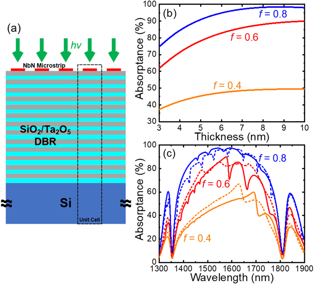
Figure 1.(a) Cross-section schematic diagram of the NbN SMSPD. From top to bottom, optical stacks correspond to a NbN microstrip, a 13-layer
According to the simulation, the SMSPDs are designed with a fixed 1 μm width and a varied of 0.4–0.8. To reduce the current crowding effect, the detectors are patterned with a double spiral strip configuration based on previous studies [25,26]. As a comparison, different geometrical configurations [see Figs. 2(a)–2(d)] are also designed with the same width on one wafer, including a short micro bridge (called Bridge), a modified double spiral strip (called Spiral-1), a regular double spiral strip (called Spiral-2), and a conventional meandered strip (called Meander). The difference between Spiral-1 and Spiral-2 is the geometry of central parts due to the different radius of curvature used. The of the microstrips mentioned is with an active area of 50 μm in diameter or a side length of 50 μm. One limitation of the double spiral strip configuration is that a photon-insensitive zone appears in the center, owing to the use of a wider strip to optimize corner curvature. To maximize the coupling efficiency, the detector can be coupled using a lens fiber (small laser beam waist) with an eccentric alignment. Other methods for optimizing the device structure to reduce the current crowding effect will be shown in a separate study.
![]()
Figure 2.Layouts [top panels, (a)–(d)] and magnified SEM images [bottom panels, (e)–(h)] of four different SMSPDs: (a) and (e), the short micrometer bridge; (b) and (f), the modified double spiral strip; (c) and (g), the regular double spiral strip; (d) and (h), the conventional meandered strip. The
For fabricating SMSPDs, a 7 nm thick NbN film is deposited on a 2 inch (5.08 cm) DBR wafer, using reactive DC magnetron sputtering in a mixture of Ar and gases. To improve the IDE of NbN microstrips, He ion irradiation is conducted to the NbN-covered wafer in a 300 mm medium-current ion implanter through a He ion energy of 20 keV at room temperature [27]. The ion irradiation fluence was empirically. Then the irradiated NbN film was processed to form the designed patterns using electron beam lithography and reactive ion etching (RIE). Figures 2(e)–2(h) show the magnified scanning electron microscope (SEM) images of the four different patterns. The coplanar waveguide electrodes were finally fabricated using ultraviolet lithography and RIE.
3. MEASUREMENTS AND RESULTS
The SMSPDs are characterized at two different base temperatures: (1) 0.84 K in an adsorption refrigerator and (2) 2.1 K in a compact closed-cycle Gifford-Mcmahon (G-M) cryocooler. To prevent the SMSPDs from latching (the detector latched at the normal state) [28,29], a shunted resistor is connected in parallel to the SMSPD chip through wire bonding. We chose a shunt resistor of (measured at room temperature), which showed optimal performance in IDE and output voltage magnitude. The detector was then biased and read out through a cryogenic coaxial cable, connecting to a DC and RF output port of a bias tee (ZX85-12G-S+, Mini Circuit Inc.) placed at room temperature. Specifically, the bias current was supplied through the DC port of the bias tee, which connected with a series resistor of 20 kΩ and an isolated DC voltage source (SIM928, SRS Inc.). In the RF port, the voltage pulse generated by the SMSPD was amplified using a 50 dB low-noise amplifier (LNA-650, RF Bay Inc.) and then fed into a pulse counter (SR400, SRS Inc.).
Figure 3(a) shows the sweeping current-voltage (I-V) curves for the chip connected with (blue line) or without (red line) a shunt resistor. It can be observed that with a shunt resistor, the nominal switching current () is increased from 66 to 80 μA. In the low-voltage region ( to 0.4 mV), the I-V curve demonstrated a slope, which corresponded to a contact resistance. Because the nominal is influenced by the shunt resistor, we first screened the devices without the shunt resistor. Figure 3(b) shows the comparison of the four different SMSPD configurations on the same wafer with a fabricated width of , measured at 2.1 K. For the , at least five samples are tested for each pattern. The average of the Bridge, Spiral-1, and Spiral-2, are , , and , respectively, while that of the Meander is only ( of those of the Spiral-1). Here the number after the symbol “” of switching currents was referred to as a standard deviation, which was estimated from the measurements of different samples. This result confirmed that the sample with a double spiral structure can effectively reduce the current crowding effect and thus guarantee a higher (IDE). Therefore, in the following experiment, a modified double spiral strip (Spiral-1) configuration is characterized due to the higher .
![]()
Figure 3.(a) Current and voltage (
The optical-electrical performances of the SMSPDs are further characterized based on the reported setup and methods [4]. Specifically, in the SDE measurements, a high-precision optical power meter (81624B, Keysight Inc.) was adopted to calibrate the input power and the attenuation of the attenuators (81570A, Keysight Inc.). A polarization controller was used to adjust the polarization of the input light. We calibrated the input power using the same optical path through switching the input fiber splicing to a fiber jumper connected with the power meter (called the monitor port) or to the fiber connected to detector under test (called the detector port). Both fiber jumpers were ended with an antireflection-coated facet, which was optimized around 1550 nm to reduce the reflectance (less than 0.3%). A continuous-wave laser (81940A, Keysight Inc., 1520–1630 nm) was used as the light source. The final input power () corresponded to a photon flux of . The power-calibrated fiber jumper was cut and spliced to the detector port. To ensure the power stability, after the measurement, the fiber to the detector port was cut and respliced to the monitored port, which showed no obvious changes in the power. The typical spliced loss was less than , which was included in the SDE (a bad splicing would result in a degraded SDE). SDE was determined by the expression of SDE = (CR-DCR)/IPR, where CR is the response count rate, DCR is the dark count rate, and IPR is the input photon rate. The DCR was an average of the CR collected for 10 s when the light was blocked by the shutter.
Then we analyzed the SDE uncertainties of our measurements. Assuming all of the sources of measurement uncertainties were independent, the total measurement uncertainty of SDE was mainly contributed by three factors and could be expressed as . Here is the relative uncertainty of the power meter (81624B), calibrated by Physikalisch-Technische Bundesanstalt (PTB); is the uncertainty of the input laser power (81940A), monitored in a measurement period; is the uncertainty of two cascaded attenuators (81570A). Thus, based on the above parameters, the was approximately .
Figure 4 shows the comparison of the SDEs versus bias current () for the SMSPDs fabricated with irradiated (called chip “irradiated”) and unirradiated (called chip “unirradiated”) NbN thin films. Both chips have the same film thickness (, deposited on the same batch) and the same geometrical configuration (1 μm wide, , and a diameter of 50 μm, Spiral-1 type). The chips were cooled in the 2.1 K G-M cryocooler and were both connected with a shunt resistor and coupled with a lens SMF. The input photon flux was at the wavelength of 1550 nm. Owing to the mentioned photon-insensitive zone in the center ( in diameter), the SMF was eccentrically aligned to maximize the coupling efficiency. Notably, the maximum SDEs of the SMSPDs fabricated with irradiated and unirradiated NbN thin films are and , respectively. via irradiation was reduced to of the unirradiated value, mainly due to the reduction of electron density of states in Femi level () [30].
![]()
Figure 4.Comparison of SDE (solid scatters) and DCR (open scatters) of the SMSPDs fabricated with irradiated and unirradiated NbN thin films as a function of bias current (
To explain the significantly enhanced IDE of the irradiated SMSPD, the physical parameters of the SMSPDs fabricated with unirradiated and irradiated NbN thin films (Spiral-1 type) were characterized as shown in Table 1. It can be found that the square resistance () was increased and the critical temperature () was suppressed in the irradiated samples, both of which would result in a larger hotspot formation in the microstrip [19]. A larger hotspot size would help reduce the detection current of the SMSPD. The detection current was referred to as a threshold bias current where the absorbed photon drives the superconducting strip to the resistive state [19]. A similar phenomenon was also observed for the irradiated nanowires [27]. Meanwhile, a ratio of at 2.1 K for the unirradiated microstrip was deduced by using the approximate expression of [31]. Here is the operating temperature, is the strip width, is the superconducting gap at 0 K, and is the electron charge. The electron diffusion coefficient [32] was estimated from the slope of the curve for the SMSPDs with or without irradiation, where is the upper critical magnetic field. This ratio of for irradiated samples slightly raised to at the same . Thus, it is speculated that a combined mechanism may play a role that involves the larger hotspot formation and higher close to the due to the ion irradiation effect. Additionally, the results of irradiated samples show that the NbN film currently used in our laboratory is not suitable to achieve high IDE SMSPD in the near infrared. Deeper analysis of the changes in the physical properties of the film via irradiation will provide us with guidance for preparing films suitable for SMSPD. Both issues will be explored in another study. Parameters of the SMSPDs Fabricated with Unirradiated and Irradiated NbN Thin Films The Samples Unirradiated 839 7.14 0.44 185 161.5 101.1 0.63 Irradiated 1036 6.40 0.50 119 100.5 66.0 0.66
It is worth noting that SMF coupling in this experiment had a large tolerance for the misalignment errors because of the small beam size and the large enough active area. We checked the alignment using an inverted microscope connected with an infrared camera at room temperature. We also confirmed the alignment indirectly by measuring the SDE of the detectors. After the cooling system returned to room temperature, we rechecked the alignment and observed no obvious shift of the laser spot.
Empirically, lowering the operating temperature would help improve the IDE of the SMSPD. Figure 5(a) shows the temperature dependence of our best irradiated SMSPD coupling with the lens SMF. The SDE (solid scatters) and DCR (open scatters) of the irradiated SMSPD (Spiral-1 type) as a function of are recorded at 2.1 K and 0.84 K, respectively. At 0.84 K, near saturation of SDE appears at the high current region, implying near-unity IDE. A maximum SDE of 92.2% at a DCR of 200 cps is obtained at 1550 nm wavelength. The measured SDE data are fitted at 0.84 K with the sigmoid function (dashed line), showing the saturation trend of the SDE with the current increase. The polarization controller was adjusted to study the polarization sensitivity of the detector as shown in Fig. 5(b). The PER (ratio between the maximum and minimum SDEs) of the “irradiated” chip shows a value of less than 1.03, consistent with the simulation () at 1550 nm. Low polarization sensitivity is preferred in many applications, e.g., providing a high SDE for the MMF-coupled systems.
![]()
Figure 5.(a) Bias current dependences of SDE and DCR of the SMSPD (“irradiated” chip), measured at two different temperatures, with 1550 nm light illumination. (b) Maximum (solid sphere) and minimum (solid square) SDEs measured at two different polarizations of light at 0.84 K. Inset: a microscope image of the SMSPD with an active area of 50 μm in diameter. Dashed lines are sigmoid function fits in both figures.
Furthermore, we measured the intrinsic DCR of the best irradiated SMSPD with and without shunt. To characterize the intrinsic DCR, the coupled fiber was removed, and the chip package block was shielded by aluminum tape to isolate any optical radiation. It was found that, without the shunt, the detector latched and could not produce stable count rate. With the shunt, as shown with triangular dots in Fig. 6, the intrinsic DCR of the SMSPD increased exponentially with current, similar to the behavior of an SNSPD with a shunt.
![]()
Figure 6.DCR of the best SMSPD with and without fiber (i.e., the intrinsic DCR) as a function of the normalized bias current (
Note that the false DCRs were observed in the region, which was removed from Fig. 6 to avoid misunderstanding (see Discussion section for more details). These false DCRs were caused by the RF oscillations due to the use of a shunt resistor [33]. However, when the detectors were biased at the same normalized current below , we did not observe obvious increase of the intrinsic DCR due to the shunt, compared with the DCR of typical SNSPDs with [34] or without [35] the shunt. Also similar to the SNSPD, the SMSPD with the shunt can be biased at , where the background DCR (see the open circles in Fig. 6) was at a low level of . Such DCR performance could meet most application needs for low DCR.
Low TJ is a significant advantage of SNSPDs over the other counterpart detectors. It is interesting to determine whether the SMSPD can maintain a low TJ as well as the SNSPD. Previously, TJ in SMSPD showed a strong current dependence, and a minimum jitter of was obtained at the current where IDE saturates, measured using a 1064 nm ps laser [21]. Here we show the system TJ of the “irradiated” chip using the TCSPC module and a 1550 nm fs laser [36]. Figures 7(a) and 7(b) show the histogram of the time delay between the laser synchronization signal and output pulse of the SMSPD, recorded at high and low currents at 0.84 K, respectively. TJ was defined as the full width at half-maximum (FWHM) of the normalized counts. As shown in Fig. 7(a), the count histogram at high of () was fitted well by the Gaussian distribution, which produced a TJ of 47.5 ps. However, in Fig. 6(b), at the lower of (), the TJ increased to 142.4 ps, where the count histogram shows a non-Gaussian shape with a “shoulder.” The “shoulder” can be regarded as the superposition of the main and secondary peaks as shown by the fit curves [green and orange lines in Fig. 7(b)]. A recent theoretical model has reproduced the non-Gaussian shape by using a modified time-dependent Ginzburg–Landau equation [37]. The mechanism was associated with the position-dependent vortex dynamics and the existence of fast and slow absorption sites across the superconducting strip. At the low current, the vortices and antivortices move slower, leading to increased delay time and thus increasing TJ. Figure 7(c) presents the current dependence of the TJ. Generally, the TJ decreases with the increase of the current. However, at the currents where the IDE changes rapidly (e.g., 72–84 μA, light orange region in the figure), an inflection point of TJ appears in this current region, which may be caused by the effects of the non-Gaussian shape. The arrows in the figure mark two specific currents, at which Figs. 7(a) and 7(b) are reordered.
![]()
Figure 7.Histogram of time-correlated photon counts measured at 1550 nm. (a)
A minimum system jitter of for our SNMPDs was obtained at . We believe this relatively large system jitter in our experiment was because of the relatively large electrical noise jitter as well as the geometrical jitter. Specifically, because the SMSPD was shunted with a small resistor, the output pulse amplitude was significantly reduced from 2 to , resulting in a lower slope of the rising edge of the response pulse. This produced a relatively large electrical noise jitter with a magnitude of [36,38]. Besides, the 50 μm diameter active area would produce a geometrical jitter with a magnitude of [39,40]. In the future, it would be interesting to explore the physical limit of the time jitter of SMSPD using cryogenic amplifiers and shorter strips.
Figure 8 shows more details of the “irradiated” chip. Figure 8(a) shows the photon-response pulse of the SMSPD, with a fitted decay time (1/e criterion) of for the falling edge of the pulse. Although shunted with a resistor, a high pulse magnitude of was observed, guaranteeing a good signal-to-noise ratio of the output pulse. Figure 8(b) shows the CR dependence of the SDE measured at at 0.84 K. A CR of at the 3 dB cutoff point of the SDE was obtained, while a maximum CR (MCR) of was determined at the SDE of 10%. The measured MCR was generally less than the MCR deduced from the decay time [1/(36 ns) ], possibly owing to the limitation of our currently used AC-coupled readout circuit [40]. However, the advantage of SMSPD is that when the active area is large, there is no notable overshoot effect in the falling edge of the pulse caused by large kinetic inductance [41]. Figure 8(c) shows the wavelength dependence of the SDE at TE polarization at at 0.84 K. In the wavelength range of 1520 to 1630 nm, the SDE shows a value greater than 88%. Because the difference between the peak and dip values of the simulated absorptance in this wavelength range is , which is close to the measurement error of the SDE, it is difficult to observe a clear dip (around 1570 nm) in the SDE. When the wavelength is longer than 1590 nm, the SDE demonstrates a slight decrease with the increase of the wavelength because of the non-saturation of the SDEs at the longer wavelength.
![]()
Figure 8.(a) Oscilloscope single pulse waveform graph of response versus time. The exponential fitting of the falling edge is given as 36 ns. (b) The dependence of SDE and count rate of SMSPD at 0.84 K. The count rate is
Figure 8(d) demonstrates the performance of our device coupled with a lens MMF with a core diameter of 50 μm and a beam waist of . The MMF-coupled SDE versus was recorded at two different photon fluxes ( and , respectively). It was found that the SDE recorded at the low photon flux () was fluctuating at the high bias current region () due to the fluctuation of the large DCR. A sigmoid fit was plotted against these experimental data, showing the trend of the SDE() curve. The maximum SDEs under these two photon fluxes were and 63%, respectively, determined at . The slight increment of in the SDE confirmed there was a weak blocking effect at high count rate. However, the maximum SDE was still lower than expectation. We speculated that the relatively low SDE of the MMF coupling in this experiment was mainly attributed to a relatively large misalignment of the laser spot due to the lack of clear alignment marks in the field of view. In the future, we would fabricate auxiliary alignment marks on the SMSPDs, similar to what we have done in SNSPDs [4], which would further improve the alignment accuracy. However, according to our knowledge, this SDE is still the highest value reported for the MMF-coupled detectors at 1550 nm. Meanwhile, owing to the broadband background radiation transmitted by the MMF coupling, a significantly raised DCR was observed, which can be suppressed using cold narrowband filters, e.g., an MMF-coupled filter bench [42]. Through Gaussian fitting, TJ of at is obtained, which is slightly larger than that of the SMF coupling due to the fiber-associated dispersion in optical signal transmission in MMF [43].
Finally, the SMSPD performances are compared with the state of the art of the SNSPDs at 1550 nm wavelength listed in Table 2, showing the potential of the SMSPD. The SNSPD with an active area of 50 μm diameter and operated at 1550 nm usually demonstrates a very large kinetic inductance (i.e., a long decay time over 1 μs without a series resistor), large TJ, and a very low yield (based on our own experience for NbN detectors). In contrast, the SMSPD with the same size exhibits an improved decay time, TJ, and yield [ (14/21) in one wafer, with a criterion of without shunt], making it attractive for applications requiring a large active area, high timing performance, and efficient detection. Comparison of the Key Merits of the SNSPDs and SMSPDs Operated at 1550 nm Wavelength Use of a low temperature amplifier. Not identical to the rest time, due to the influence of the shunt resistor.Detectors Material Width SMF Coupling MMF Coupling Decay SDE (%) DCR (cps) TJ (ps) PER SDE (%) DCR (cps) TJ (ps) SNSPD 80 98.0 1.23 N/A N/A N/A WSi [ 120 93.2 150 1.16 N/A N/A N/A NbN [ 75 92.1 40 3.5 N/A N/A N/A 70 75 18.7 3.75 50 N/A N/A SMSPD 1000 N/A N/A N/A N/A N/A WSi [ 2000 N/A N/A N/A N/A N/A N/A NbN [ 1000 35 at 1.3 μm 45 N/A N/A N/A N/A 2.5 NbN (this paper) 1000 92.2 47.5 1.03 63 50 36
4. DISCUSSIONS
Here we provide more insights and discussions to our results. First, for optical cavity design, recent simulation and experiment results (e.g., Refs. [2,4] and this paper) have shown that near unity absorptance and SDE can be obtained without the additional layers stacked on the top of the NbN strip, because of the formation of a strong half-wave cavity. Adding the additional layer on the top of the NbN strip would result in a narrower resonated bandwidth but with no obvious enhancement in absorptance. Therefore, to simplify the fabrication process, we did not fabricate the additional dielectric layers. Second, for the strip geometry, we have simulated strips with varied widths (e.g., 1–3 μm) and varied filling factors (e.g., 0.3–0.97). It was found that with each strip width it was possible to achieve a maximum absorptance close to 100%. For instance, we show a comparison of the simulated absorptance for micro strips with widths of 1 and 3 μm at specific filling factors in Fig. 9. A maximum absorptance over 95% was obtained at both of these strip geometrical structures. Therefore, the choice of strip width mainly depends on the processing accuracy and the actual requirements. In this study, the use of 1 μm wide strips with a varied of 0.4–0.8 was empirical. Third, the double spiral strip configuration was useful to improve the maximum bias current. However, as pointed out earlier, it has a drawback that it is insensitive to detection in the middle and thus requires more sensitive alignment and results in wasting of the SMSPD active area. Thus, we thought the spiral strip configuration would be useful for the case in which the SMSPDs have a very large active area and are coupled to a beam with a large beam size. Thus, the middle insensitive area would sacrifice a very small part of the SDE. For example, considering a very large active detector with a 10 μm diameter insensitive area coupled to a 150 μm diameter Gaussian beam, the estimated coupling loss was . Besides, recent advances in reducing the effect of current crowding have been made, such as thickening the turns of the meander strip [44].
![]()
Figure 9.Simulated wavelength dependence of optical absorptance for microstrips with two different widths (
In our experiments, the SMSPD was shunted with a resistor, which would cause the RF oscillations at the greater than (up to , empirically), where the detector suffered from the RLC (resistance, inductance, and capacitance series circuit) oscillations. This phenomenon was also observed in the SNSPD shunted with a resistor [33]. In this current region, the pulse waveform of the RF oscillations observed by the oscilloscope was stable and repeated at a specific frequency, which was easy to distinguish from the normal photon response of the detector. Furthermore, in the DCR measurement, the DCR logarithmically increases with the bias current. However, after entering the RF oscillation region, the curve of the DCR versus would show a different slope, which provides evidence for us to distinguish the normal operation region from the RF oscillation region. It is worth noting that, generally, our detectors are biased below the switching current, and the RF oscillations would not affect the detector’s performance. Moreover, in the low bias current region (below ), we also did not observe obvious RF oscillations induced by the shunt (implied by a theoretical prediction in Ref. [37]), through monitoring the periods of the pulse of the dark count. We speculated this type of RF oscillations to have either possibly occurred at specific kinetic inductance, shunt resistor, and strip width, or they were too weak to observe.
In terms of detection mechanism, we adopted a simplified diffusion hotspot model [45] to further explain the SDE enhancement caused by ion irradiation. This model describes the photon response of a superconducting strip through an analytical expression of , where is a minimum energy (or corresponding to a cutoff wavelength ) detectable by the superconducting strip, is the speed of light, is the time scale of the quasiparticle multiplication process, and is multiplication efficiency of quasiparticles [46]. According to the data of our electrical transport measurements, the ion irradiation was found to affect the related physical parameters of the strip (e.g., , , , ), and then the due to irradiation was estimated using the change ratio of these parameters. Via calculation, was reduced to nearly 65% of its unirradiated value. Correspondingly, the was extended to longer wavelength, which implied an enhanced spectral sensitivity.
Recent theoretical works have extended the analytical hotspot model to more complicated models [19,47], which require numerical simulations. For example, the calculation by Vodolazov [19] based on a hotspot two-temperature model (assuming a short thermalization time at the initial stage of hotspot formation) predicted the single-photon detection ability of the strip with a microscale width, when the maximal detection current () exceeded a specific ratio of . Here we compared the detection current of our devices with the theoretical results shown in Vodolazov’s paper [19]. First, we determined the of our device through measuring the normalized detection efficiency (NDE) as a function of , illuminated at a specific photon energy (wavelength). As shown in Fig. 10(a), the data of the irradiated device were recorded at 0.84 K and illuminated at two different wavelengths (1064 nm and 1550 nm, respectively). From the NDE() curves, the maximal detection current () with shunt was defined as the current at which the NDE became greater than a threshold value of 0.99 (i.e., the NDE became saturated). Assuming the has the same increase ratio (, empirically) as the due to the shunt, then the was normalized to the , i.e., . We further assumed the .
![]()
Figure 10.(a) Bias current dependence of normalized detection efficiency (NDE) for the irradiated SMSPD, recorded under the 1064 nm and 1550 nm photons’ illumination, while operated at 0.84 K with a shunt resistor. Arrows indicate the locations of the
Then, according to Vodolazov’s paper [19] and our measured physical parameters (shown in Table 1) for the irradiated NbN device, we calculated the relevant physical parameters of our device in terms of Vodolazov’s paper [19]: , the characteristic energy of , where and the thickness . We also estimated the coefficient , , and the excitation photon engorgement of at 1550 (1064) nm, respectively.
Based on the abovementioned parameters, especially for the value of in our NbN device, we compared the experiment data ( versus ) with the calculated data taken from Vodolazov’s paper [19] as shown in Fig. 10(b). Two sets of the calculated data, which corresponded to two different strip widths ( and ) with the same value of , were plotted against our data. Because the and values of these data are close, the strip width would play a key role on the ratio of , when the strip was illuminated with the same photon energy. Thus, the two sets of calculated data may serve as the upper and lower boundaries for our results. However, more experiment data are needed to draw a full picture of the curve, especially for the low-energy region (corresponding to the longer wavelength ) and high-energy region (corresponding to the shorter wavelength ). These works would be done in the later experiments. It is also interesting to note, in the low-energy region (e.g., ), whether the experiment data for different strip widths would overlap each other; while in the high energy region (e.g., ), whether the ratio of would tend to saturation. Both of these studies would provide more information for the understanding of detection mechanisms.
5. CONCLUSIONS
In conclusion, this work simulated, fabricated, and characterized a NbN microstrip on a DBR substrate with various filling factors (0.4–0.8) and various strip configurations (bridge, double spiral, and meander). Simulation shows that a high filling factor is necessary to achieve high SDE in the SMSPD. A double spiral strip configuration is helpful in reducing the current crowding effect. Owing to the use of the NbN film pre-irradiated by He ions, the IDE of the NbN SMSPD is significantly improved, providing more physical insights into the detection mechanism of the SMSPD. Based on the abovementioned methods, this study successfully demonstrated the NbN SMSPD with a strip width of 1 μm, a filling factor of , and an active area of 50 μm in diameter, showing a maximum SDE of 92.2% at 1550 nm, a DCR of 200 cps, a minimum TJ of 48 ps, and a PER of 1.03 at 0.84 K. Operated in a 2.1 K closed-cycle cryocooler, the detector shows a maximum SDE of over 70% at 1550 nm. In addition, the SMSPD was further coupled with a multimode fiber, where the detector shows a maximum SDE of over 60% and a TJ of . Results of this study shed light on the development SMSPDs for efficient single-photon detection, which would show the potential application prospects in quantum optics and photon-starved LIDAR.
Acknowledgment
Acknowledgment. The authors thank Xiaoyu Liu for technical assistance in EBL and Peng Hu for technical assistance in the detector’s optical coupling. The authors also thank Huiqin Yu for technical support in the use of the 0.8 K cryostat.
References
[1] G. N. Gol’tsman, O. Okunev, G. Chulkova, A. Lipatov, A. Semenov, K. Smirnov, B. Voronov, A. Dzardanov, C. Williams, R. Sobolewski. Picosecond superconducting single-photon optical detector. Appl. Phys. Lett., 79, 705-707(2001).
[2] P. Hu, H. Li, L. You, H. Wang, Y. Xiao, J. Huang, X. Yang, W. Zhang, Z. Wang, X. Xie. Detecting single infrared photons toward optimal system detection efficiency. Opt. Express, 28, 36884-36891(2020).
[3] D. V. Reddy, R. R. Nerem, S. W. Nam, R. P. Mirin, V. B. Verma. Superconducting nanowire single-photon detectors with 98% system detection efficiency at 1550 nm. Optica, 7, 1649-1653(2020).
[4] W. Zhang, L. You, H. Li, J. Huang, C. Lv, L. Zhang, X. Liu, J. Wu, Z. Wang, X. Xie. NbN superconducting nanowire single photon detector with efficiency over 90% at 1550 nm wavelength operational at compact cryocooler temperature. Sci. China Phys. Mech. Astron., 60, 120314(2017).
[5] F. Marsili, V. B. Verma, J. A. Stern, S. Harrington, A. E. Lita, T. Gerrits, I. Vayshenker, B. Baek, M. D. Shaw, R. P. Mirin, S. W. Nam. Detecting single infrared photons with 93% system efficiency. Nat. Photonics, 7, 210-214(2013).
[6] H. Shibata, K. Shimizu, H. Takesue, Y. Tokura. Ultimate low system dark-count rate for superconducting nanowire single-photon detector. Opt. Lett., 40, 3428-3431(2015).
[7] B. Korzh, Q.-Y. Zhao, J. P. Allmaras, S. Frasca, T. M. Autry, E. A. Bersin, A. D. Beyer, R. M. Briggs, B. Bumble, M. Colangelo, G. M. Crouch, A. E. Dane, T. Gerrits, A. E. Lita, F. Marsili, G. Moody, C. Peña, E. Ramirez, J. D. Rezac, N. Sinclair, M. J. Stevens, A. E. Velasco, V. B. Verma, E. E. Wollman, S. Xie, D. Zhu, P. D. Hale, M. Spiropulu, K. L. Silverman, R. P. Mirin, S. W. Nam, A. G. Kozorezov, M. D. Shaw, K. K. Berggren. Demonstration of sub-3 ps temporal resolution with a superconducting nanowire single-photon detector. Nat. Photonics, 14, 250-255(2020).
[8] D. Y. Vodolazov. Minimal timing jitter in superconducting nanowire single-photon detectors. Phys. Rev. Appl., 11, 014016(2019).
[9] W. Zhang, J. Huang, C. Zhang, L. You, C. Lv, L. Zhang, H. Li, Z. Wang, X. Xie. A 16-pixel interleaved superconducting nanowire single-photon detector array with a maximum count rate exceeding 1.5 GHz. IEEE Trans. Appl. Supercond., 29, 2200204(2019).
[10] H. Li, Y. Wang, L. You, H. Wang, H. Zhou, P. Hu, W. Zhang, X. Liu, X. Yang, L. Zhang, Z. Wang, X. Xie. Supercontinuum single-photon detector using multilayer superconducting nanowires. Photon. Res., 7, 1425-1431(2019).
[11] F. Marsili, F. Bellei, F. Najafi, A. E. Dane, E. A. Dauler, R. J. Molnar, K. K. Berggren. Efficient single photon detection from 500 nm to 5 μm wavelength. Nano Lett., 12, 4799-4804(2012).
[12] K. J. Wei, W. Li, H. Tan, Y. Li, H. Min, W. J. Zhang, H. Li, L. X. You, Z. Wang, X. Jiang, T. Y. Chen, S. K. Liao, C. Z. Peng, F. H. Xu, J. W. Pan. High-speed measurement-device-independent quantum key distribution with integrated silicon photonics. Phys. Rev. X, 10, 031030(2020).
[13] Y. Liu, Z. W. Yu, W. Zhang, J. Y. Guan, J. P. Chen, C. Zhang, X. L. Hu, H. Li, C. Jiang, J. Lin, T. Y. Chen, L. You, Z. Wang, X. B. Wang, Q. Zhang, J. W. Pan. Experimental twin-field quantum key distribution through sending or not sending. Phys. Rev. Lett., 123, 100505(2019).
[14] H.-S. Zhong, H. Wang, Y.-H. Deng, M.-C. Chen, L.-C. Peng, Y.-H. Luo, J. Qin, D. Wu, X. Ding, Y. Hu, P. Hu, X.-Y. Yang, W.-J. Zhang, H. Li, Y. Li, X. Jiang, L. Gan, G. Yang, L. You, Z. Wang, L. Li, N.-L. Liu, C.-Y. Lu, J.-W. Pan. Quantum computational advantage using photons. Science, 370, 1460-1463(2020).
[15] T. Polakovic, W. Armstrong, G. Karapetrov, Z. E. Meziani, V. Novosad. Unconventional applications of superconducting nanowire single photon detectors. Nanomaterials, 10, 1198(2020).
[16] Y. Hochberg, I. Charaev, S. W. Nam, V. Verma, M. Colangelo, K. K. Berggren. Detecting sub-GeV dark matter with superconducting nanowires. Phys. Rev. Lett., 123, 151802(2019).
[17] L. Xue, Z. Li, L. Zhang, D. Zhai, Y. Li, S. Zhang, M. Li, L. Kang, J. Chen, P. Wu, Y. Xiong. Satellite laser ranging using superconducting nanowire single-photon detectors at 1064 nm wavelength. Opt. Lett., 41, 3848-3851(2016).
[18] C. M. Natarajan, M. G. Tanner, R. H. Hadfield. Superconducting nanowire single-photon detectors: physics and applications. Supercond. Sci. Technol., 25, 063001(2012).
[19] D. Y. Vodolazov. Single-photon detection by a dirty current-carrying superconducting strip based on the kinetic-equation approach. Phys. Rev. Appl., 7, 034014(2017).
[20] Y. P. Korneeva, D. Y. Vodolazov, A. V. Semenov, I. N. Florya, N. Simonov, E. Baeva, A. A. Korneev, G. N. Goltsman, T. M. Klapwijk. Optical single-photon detection in micrometer-scale NbN bridges. Phys. Rev. Appl., 9, 064037(2018).
[21] N. N. Manova, E. O. Smirnov, Y. P. Korneeva, A. A. Korneev, G. N. Goltsman. Superconducting photon counter for nanophotonics applications. J. Phys. Conf. Ser., 1410, 012147(2019).
[22] I. Charaev, Y. Morimoto, A. Dane, A. Agarwal, M. Colangelo, K. K. Berggren. Large-area microwire MoSi single-photon detectors at 1550 nm wavelength. Appl. Phys. Lett., 116, 242603(2020).
[23] J. Chiles, S. M. Buckley, A. Lita, V. B. Verma, J. Allmaras, B. Korzh, M. D. Shaw, J. M. Shainline, R. P. Mirin, S. W. Nam. Superconducting microwire detectors based on WSi with single-photon sensitivity in the near-infrared. Appl. Phys. Lett., 116, 242602(2020).
[24] Y. Korneeva, D. Vodolazov, I. Florya, N. Manova, E. Smirnov, A. Korneev, M. Mikhailov, G. Goltsman, T. M. Klapwijk. Single photon detection in micron scale NbN and α-MoSi superconducting strips. EPJ Web Conf., 190, 04010(2018).
[25] J. Huang, W. J. Zhang, L. X. You, X. Y. Liu, Q. Guo, Y. Wang, L. Zhang, X. Y. Yang, H. Li, Z. Wang, X. M. Xie. Spiral superconducting nanowire single-photon detector with efficiency over 50% at 1550 nm wavelength. Supercond. Sci. Technol., 30, 074004(2017).
[26] I. Charaev, A. Semenov, S. Doerner, G. Gomard, K. Ilin, M. Siegel. Current dependence of the hot-spot response spectrum of superconducting single-photon detectors with different layouts. Supercond. Sci. Technol., 30, 025016(2017).
[27] W. Zhang, Q. Jia, L. You, X. Ou, H. Huang, L. Zhang, H. Li, Z. Wang, X. Xie. Saturating intrinsic detection efficiency of superconducting nanowire single-photon detectors via defect engineering. Phys. Rev. Appl., 12, 044040(2019).
[28] M. W. Brenner, D. Roy, N. Shah, A. Bezryadin. Dynamics of superconducting nanowires shunted with an external resistor. Phys. Rev. B, 85, 224507(2012).
[29] E. Toomey, Q.-Y. Zhao, A. N. McCaughan, K. K. Berggren. Frequency pulling and mixing of relaxation oscillations in superconducting nanowires. Phys. Rev. Appl., 9, 064021(2018).
[30] J. Y. Juang, D. A. Rudman, J. Talvacchio, R. B. van Dover. Effects of ion irradiation on the normal state and superconducting properties of NbN thin films. Phys. Rev. B, 38, 2354-2361(1988).
[31] J. R. Clem, V. G. Kogan. Kinetic impedance and depairing in thin and narrow superconducting films. Phys. Rev. B, 86, 174521(2012).
[32] A. Semenov, B. Gunther, U. Bottger, H. W. Hubers, H. Bartolf, A. Engel, A. Schilling, K. Ilin, M. Siegel, R. Schneider, D. Gerthsen, N. A. Gippius. Optical and transport properties of ultrathin NbN films and nanostructures. Phys. Rev. B, 80, 054510(2009).
[33] D. K. Liu, S. J. Chen, L. X. You, Y. L. Wang, S. Miki, Z. Wang, X. M. Xie, M. H. Jiang. Nonlatching superconducting nanowire single-photon detection with quasi-constant-voltage bias. Appl. Phys. Express, 5, 125202(2012).
[34] S. Miki, T. Yamashita, H. Terai, Z. Wang. High performance fiber-coupled NbTiN superconducting nanowire single photon detectors with Gifford-McMahon cryocooler. Opt. Express, 21, 10208-10214(2013).
[35] T. Yamashita, S. Miki, K. Makise, W. Qiu, H. Terai, M. Fujiwara, M. Sasaki, Z. Wang. Origin of intrinsic dark count in superconducting nanowire single-photon detectors. Appl. Phys. Lett., 99, 161105(2011).
[36] L. X. You, X. Y. Yang, Y. H. He, W. X. Zhang, D. K. Liu, W. J. Zhang, L. Zhang, L. Zhang, X. Y. Liu, S. J. Chen, Z. Wang, X. M. Xie. Jitter analysis of a superconducting nanowire single photon detector. AIP Adv., 3, 072135(2013).
[37] D. Y. Vodolazov, N. N. Manova, Y. P. Korneeva, A. A. Korneev. Timing jitter in NbN superconducting microstrip single-photon detector. Phys. Rev. Appl., 14, 044041(2020).
[38] J. J. Wu, L. X. You, S. J. Chen, H. Li, Y. H. He, C. L. Lv, Z. Wang, X. M. Xie. Improving the timing jitter of a superconducting nanowire single-photon detection system. Appl. Opt., 56, 2195-2200(2017).
[39] N. Calandri, Q.-Y. Zhao, D. Zhu, A. Dane, K. K. Berggren. Superconducting nanowire detector jitter limited by detector geometry. Appl. Phys. Lett., 109, 152601(2016).
[40] A. J. Kerman, D. Rosenberg, R. J. Molnar, E. A. Dauler. Readout of superconducting nanowire single-photon detectors at high count rates. J. Appl. Phys., 113, 144511(2013).
[41] C. Zhang, W. Zhang, J. Huang, L. You, H. Li, C. Lv, T. Sugihara, M. Watanabe, H. Zhou, Z. Wang, X. Xie. NbN superconducting nanowire single-photon detector with an active area of 300 μm-in-diameter. AIP Adv., 9, 075214(2019).
[42] C. Zhang, W. Zhang, L. You, J. Huang, H. Li, X. Sun, H. Wang, C. Lv, H. Zhou, X. Liu, Z. Wang, X. Xie. Suppressing dark counts of multimode-fiber-coupled superconducting nanowire single-photon detector. IEEE Photon. J., 11, 7103008(2019).
[43] J. Chang, I. E. Zadeh, J. W. N. Los, J. Zichi, A. Fognini, M. Gevers, S. Dorenbos, S. F. Pereira, P. Urbach, V. Zwiller. Multimode-fiber-coupled superconducting nanowire single-photon detectors with high detection efficiency and time resolution. Appl. Opt., 58, 9803-9807(2019).
[44] R. Baghdadi, E. Schmidt, S. Jahani, I. Charaev, M. G. W. Müller, M. Colangelo, D. Zhu, K. Ilin, A. D. Semenov, Z. Jacob, M. Siegel, K. K. Berggren. Enhancing the performance of superconducting nanowire-based detectors with high-filling factor by using variable thickness. Supercond. Sci. Technol., 34, 035010(2021).
[45] A. Semenov, A. Engel, H. W. Hubers, K. Il’in, M. Siegel. Spectral cut-off in the efficiency of the resistive state formation caused by absorption of a single-photon in current-carrying superconducting nano-strips. Eur. Phys. J. B, 47, 495-501(2005).
[46] A. Engel, A. Schilling. Numerical analysis of detection-mechanism models of superconducting nanowire single-photon detector. J. Appl. Phys., 114, 214501(2013).
[47] A. Engel, J. J. Renema, K. Ilin, A. Semenov. Detection mechanism of superconducting nanowire single-photon detectors. Supercond. Sci. Technol., 28, 114003(2015).

Set citation alerts for the article
Please enter your email address
© Copyright 2018-2021 | Chinese Laser Press. All Rights Reserved 沪ICP备15018463号-20