
Guang Zhu, Yuehua Huo, Yanqiong Shi. Switchable Broadband Terahertz Absorber Based on Temperature Control[J]. Laser & Optoelectronics Progress, 2021, 58(13): 1316001
- Laser & Optoelectronics Progress
- Vol. 58, Issue 13, 1316001 (2021)
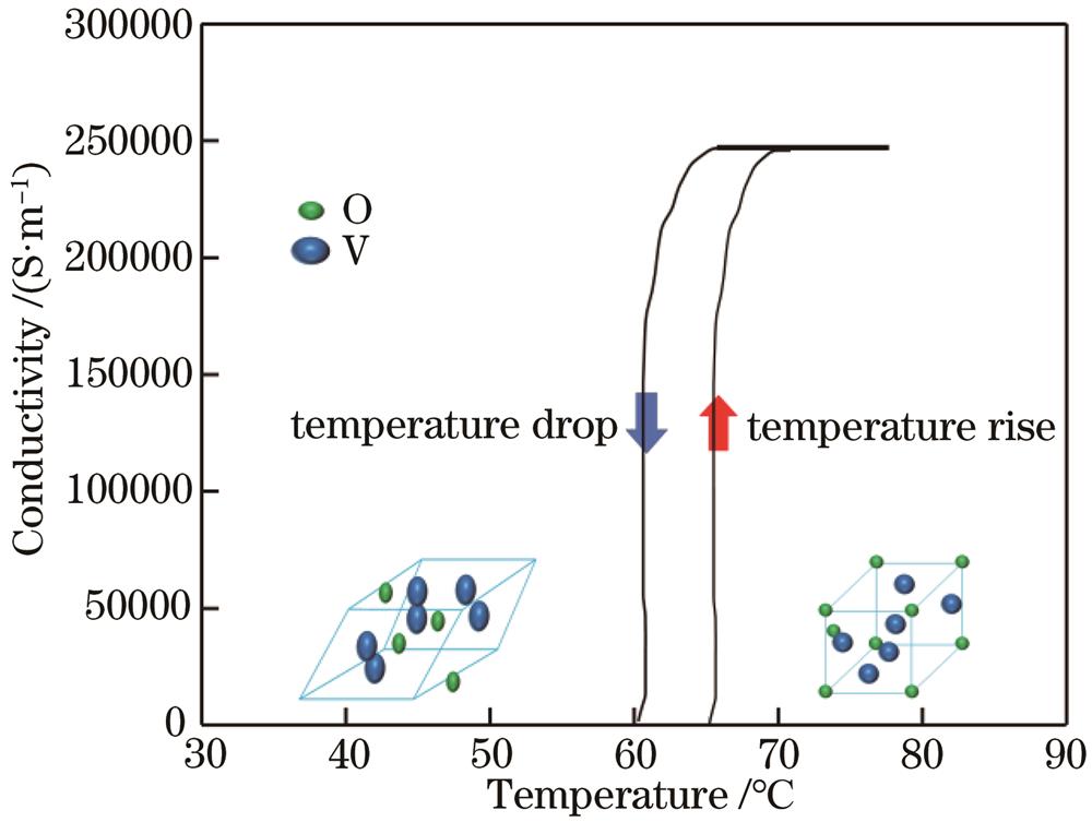
Fig. 1. Changes in conductivity and crystal structure of VO2 at different temperatures
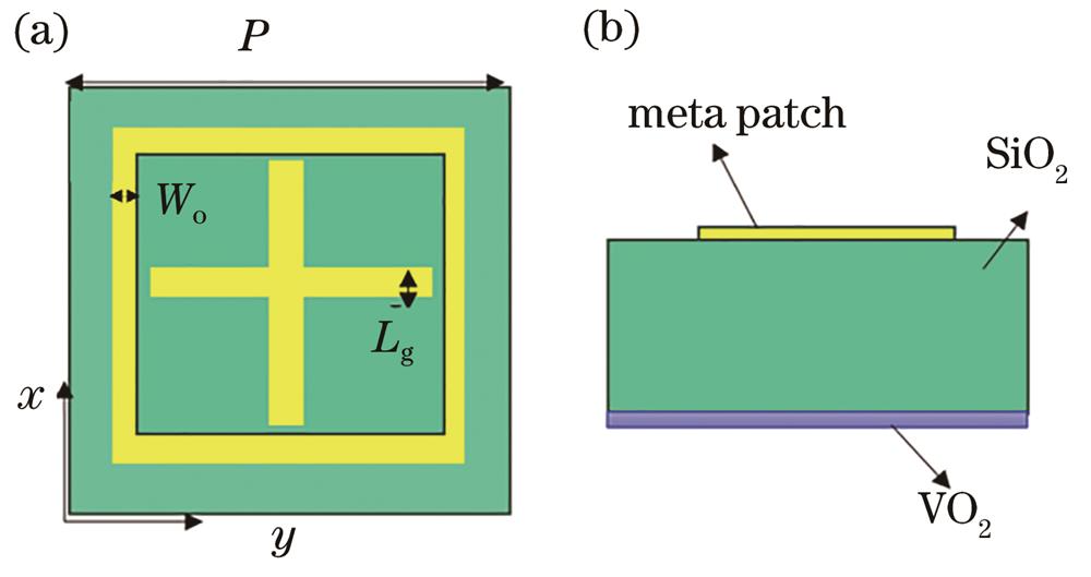
Fig. 2. Switchable broadband absorber structure diagram. (a) Top view; (b) side view
Fig. 3. Changes of absorption efficiencies under different conductivities
Fig. 4. The real part of the permittivity at different conductivities
Fig. 5. The imaginary part of the permittivity at different conductivities
Fig. 6. The real part and imaginary part of relative impedance and absorption efficiency curve of absorber under high temperature conditions
Fig. 7. The real part of the surface relative impedance at different conductivities
Fig. 8. The imaginary part of the surface relative impedance at different conductivities
Fig. 9. The transmission, absorption, and reflection curves of the adjustable broadband absorber under the vertical incidence of electromagnetic waves in the metal state
Fig. 10. Absorption curves at different polarization angles
Fig. 11. Absorption curves at different incident angles in TE mode
Fig. 12. Absorption curves at different incident angles in TM mode
|
Table 1. Conductivity of VO2 resistive film at different temperatures

Set citation alerts for the article
Please enter your email address
© Copyright 2018-2021 | Chinese Laser Press. All Rights Reserved 沪ICP备15018463号-20