• Photonics Research
  • Vol. 8, Issue 7, 1243 (2020)
Ke Jiang1、2, Xiaojuan Sun1、2、6、*, Zi-Hui Zhang1、3, Jianwei Ben1、2、5, Jiamang Che3, Zhiming Shi1、2, Yuping Jia1、2, Yang Chen1、2, Shanli Zhang1、2, Wei Lv1、4, and Dabing Li1、2、7、*
Author Affiliations
  • 1State Key Laboratory of Luminescence and Applications, Changchun Institute of Optics, Fine Mechanics and Physics, Chinese Academy of Sciences, Changchun 130033, China
  • 2Center of Materials Science and Optoelectronics Engineering, University of Chinese Academy of Sciences, Beijing 100049, China
  • 3Key Laboratory of Electronic Materials and Devices of Tianjin, School of Electronics and Information Engineering, Hebei University of Technology, Tianjin 300401, China
  • 4Key Laboratory of Advanced Structural Materials, Ministry of Education, Changchun University of Technology, Changchun 130012, China
  • 5Current Address: College of Materials Science and Engineering, Shenzhen University, Shenzhen 518071, China
  • 6e-mail: sunxj@ciomp.ac.cn
  • 7e-mail: lidb@ciomp.ac.cn
  • show less
    DOI: 10.1364/PRJ.392041 Cite this Article Set citation alerts
    Ke Jiang, Xiaojuan Sun, Zi-Hui Zhang, Jianwei Ben, Jiamang Che, Zhiming Shi, Yuping Jia, Yang Chen, Shanli Zhang, Wei Lv, Dabing Li. Polarization-enhanced AlGaN solar-blind ultraviolet detectors[J]. Photonics Research, 2020, 8(7): 1243 Copy Citation Text show less
    (a) Lattice diagram of hexagonal structure and origination scheme of polarization. (b), (c) Polarization variation under tensile and compressive strain. (d) Origination of interface charges due to polarization effect. (e), (f) Charge distribution and energy band diagram of AlGaN heterostructure. (g), (h) Designed devices SA and SB in simulations.
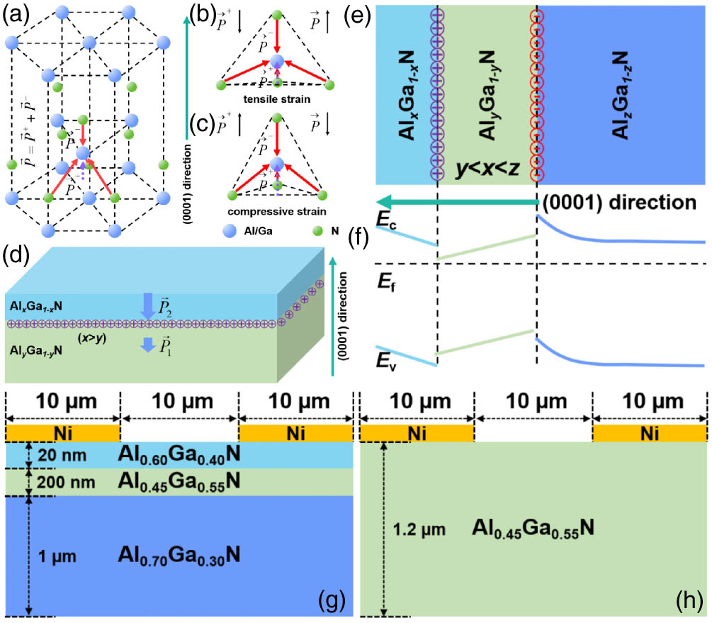
    Fig. 1. (a) Lattice diagram of hexagonal structure and origination scheme of polarization. (b), (c) Polarization variation under tensile and compressive strain. (d) Origination of interface charges due to polarization effect. (e), (f) Charge distribution and energy band diagram of AlGaN heterostructure. (g), (h) Designed devices SA and SB in simulations.
    Simulated energy-band diagram, electric field, and carrier concentration in dark and on illumination for devices (a)–(c) SA and (d)–(f) SB, respectively.
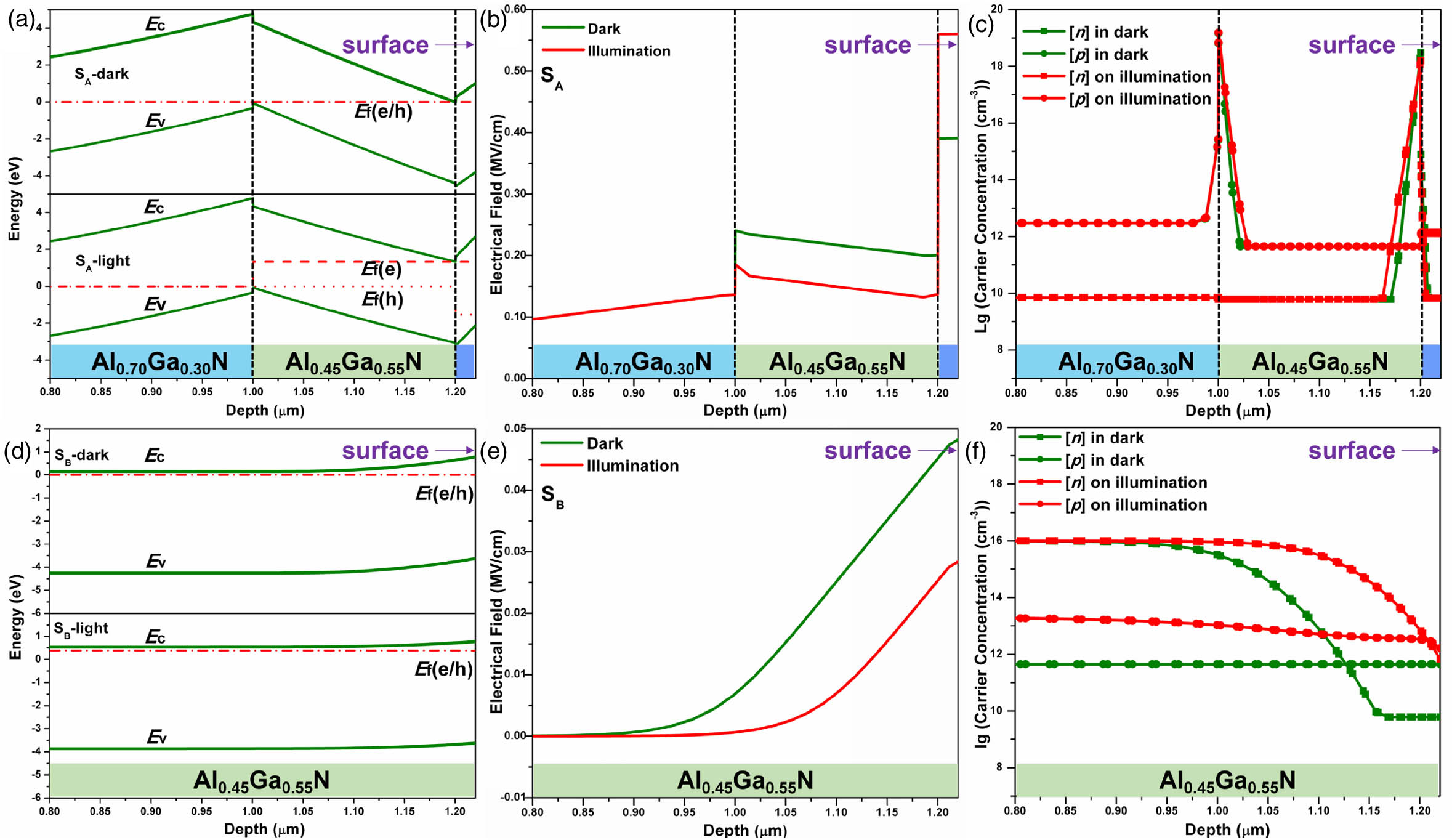
    Fig. 2. Simulated energy-band diagram, electric field, and carrier concentration in dark and on illumination for devices (a)–(c) SA and (d)–(f) SB, respectively.
    Simulated (a) IV curves in dark and on illumination and (b) spectral responses under different biases for devices SA and SB (semilog scale in the inset).
    Fig. 3. Simulated (a) IV curves in dark and on illumination and (b) spectral responses under different biases for devices SA and SB (semilog scale in the inset).
    (a) Schematic epitaxial structures of devices SA and SB. (b) Temperature and reflectance curves during the growth procedure of devices SA and SB (inset). (c), (d) XRD and XRC results of the wafers for devices SA and SB. (e) Absorption spectra of the wafers for devices SA and SB. (f) Structure diagram and electrode optical image of the fabricated devices.
    Fig. 4. (a) Schematic epitaxial structures of devices SA and SB. (b) Temperature and reflectance curves during the growth procedure of devices SA and SB (inset). (c), (d) XRD and XRC results of the wafers for devices SA and SB. (e) Absorption spectra of the wafers for devices SA and SB. (f) Structure diagram and electrode optical image of the fabricated devices.
    (a) IV curves in dark and on illumination for devices SA and SB. (b), (c) Band diagrams of devices SB and SA in dark. (d) Spectral responses of devices SA and SB (inset). (e), (f) Band diagrams of devices SB and SA on illumination. (g) Response time of devices SA and SB as a function of load resistance. Inset: Normalized transient spectra at 10 kΩ. (h) Schematic circuit to measure the transient spectra.
    Fig. 5. (a) IV curves in dark and on illumination for devices SA and SB. (b), (c) Band diagrams of devices SB and SA in dark. (d) Spectral responses of devices SA and SB (inset). (e), (f) Band diagrams of devices SB and SA on illumination. (g) Response time of devices SA and SB as a function of load resistance. Inset: Normalized transient spectra at 10  . (h) Schematic circuit to measure the transient spectra.
    (a) Band alignment and carrier distribution with high work function metal to adjust the carrier concentration. (b) Structure diagram and electrode optical image of device SC. (c) IV curves of device SC in dark and on illumination. (d) Spectral response of device SC under different biases.
    Fig. 6. (a) Band alignment and carrier distribution with high work function metal to adjust the carrier concentration. (b) Structure diagram and electrode optical image of device SC. (c) IV curves of device SC in dark and on illumination. (d) Spectral response of device SC under different biases.
    Transmittance spectrum of the Ni/Au semitransparent film.
    Fig. 7. Transmittance spectrum of the Ni/Au semitransparent film.
    Schematic plan-view of the electrodes of devices (a) SA, SB, and (b) SC.
    Fig. 8. Schematic plan-view of the electrodes of devices (a) SA, SB, and (b) SC.
    (a) C−V measurement results of the wafer for devices SA and SC. (b) Ohmic check for Hall measurements at room temperature. (c) Temperature-dependent Hall measurement results of the wafer for devices SA and SC.
    Fig. 9. (a) CV measurement results of the wafer for devices SA and SC. (b) Ohmic check for Hall measurements at room temperature. (c) Temperature-dependent Hall measurement results of the wafer for devices SA and SC.
    Ke Jiang, Xiaojuan Sun, Zi-Hui Zhang, Jianwei Ben, Jiamang Che, Zhiming Shi, Yuping Jia, Yang Chen, Shanli Zhang, Wei Lv, Dabing Li. Polarization-enhanced AlGaN solar-blind ultraviolet detectors[J]. Photonics Research, 2020, 8(7): 1243
    Download Citation