1State Key Laboratory of Luminescence and Applications, Changchun Institute of Optics, Fine Mechanics and Physics, Chinese Academy of Sciences, Changchun 130033, China
2Center of Materials Science and Optoelectronics Engineering, University of Chinese Academy of Sciences, Beijing 100049, China
3Key Laboratory of Electronic Materials and Devices of Tianjin, School of Electronics and Information Engineering, Hebei University of Technology, Tianjin 300401, China
4Key Laboratory of Advanced Structural Materials, Ministry of Education, Changchun University of Technology, Changchun 130012, China
5Current Address: College of Materials Science and Engineering, Shenzhen University, Shenzhen 518071, China
AlGaN solar-blind ultraviolet detectors have great potential in many fields, although their performance has not fully meet the requirements until now. Here, we proposed an approach to utilize the inherent polarization effect of AlGaN to improve the detector performance. AlGaN heterostructures were designed to enhance the polarization field in the absorption layer, and a high built-in field and a high electron mobility conduction channel were formed. As a result, a high-performance solar-blind ultraviolet detector with a peak responsivity of 1.42 A/W at 10 V was achieved, being 50 times higher than that of the nonpolarization-enhanced one. Moreover, an electron reservoir structure was proposed to further improve the performance. A higher peak responsivity of 3.1 A/W at 30 V was achieved because the electron reservoir structure could modulate the electron concentration in the conduction channel. The investigation presented here provided feasible approaches to improve the performance of the AlGaN detector by taking advantage of its inherent property.
1. INTRODUCTION
Solar-blind ultraviolet (SBUV) detectors can be widely applied in the scopes of short-range communication, corona discharges in transmission line and high-voltage equipment, flame detection, missile plume detection, biological imaging, etc., since they can operate on the Earth in broad daylight without any background signal from the Sun [1–5]. However, currently available SBUV detectors are mostly based on high-voltage and high-vacuum devices, which feature large volume, high energy consumption, fragility, etc. [6–10]. Therefore, there is an urgent need to renovate SBUV detection technologies. AlGaN is one of the most promising materials for SBUV detection due to its tunable ultrawide bandgap and efficient absorption in the SBUV band. The development of AlGaN materials gives rise to the fabrication of various UV detectors, including photoconductors, Schottky diodes, metal-semiconductor-metal (MSM) structures, p-n and p-i-n diodes, etc. [11–15]. However, the device performance will sharply decrease with the increase of Al content due to crystal quality deterioration and p-type doping difficulty.
Several approaches have been applied to conquer the bottlenecks. AlN/sapphire template and p-GaN were used to replace the sapphire substrate and the p-AlGaN to improve the crystal quality and p-doping efficiency [16]. Although a high peak external quantum efficiency (EQE) was achieved, the peak responsivity () was low due to the absence of internal gain and the existence of p-GaN damaged the SBUV detection characters. To avoid the p-doping difficulty, an asymmetric electrode MSM structure was proposed [17]. A self-powered SBUV detector was achieved, but the zero-bias EQE was low, too. Afterward, surface modifications were introduced to improve the MSM photodetector performance. Al nanoparticles were employed to modify the AlGaN MSM SBUV detector, and it was found that the could be enhanced due to the surface plasmon resonance (SPR) effect [18,19]. However, the SPR effect can hardly be applied inside the AlGaN structure since it decayed exponentially in the direction perpendicular to the surface and only took effect within few dozens of nanometers. Therefore, the unique 2D electron gas (2DEG) at the interface of AlGaN heterostructure was noticed [20–23]. An SBUV peak higher than could even be achieved based on the 2DEG [20,21,23], but the high visible-blind ultraviolet (VBUV) and unspecified response speed may limit their wide-range application. Hence, the performance of the AlGaN SBUV detector is still less than expected, and further improvement is required.
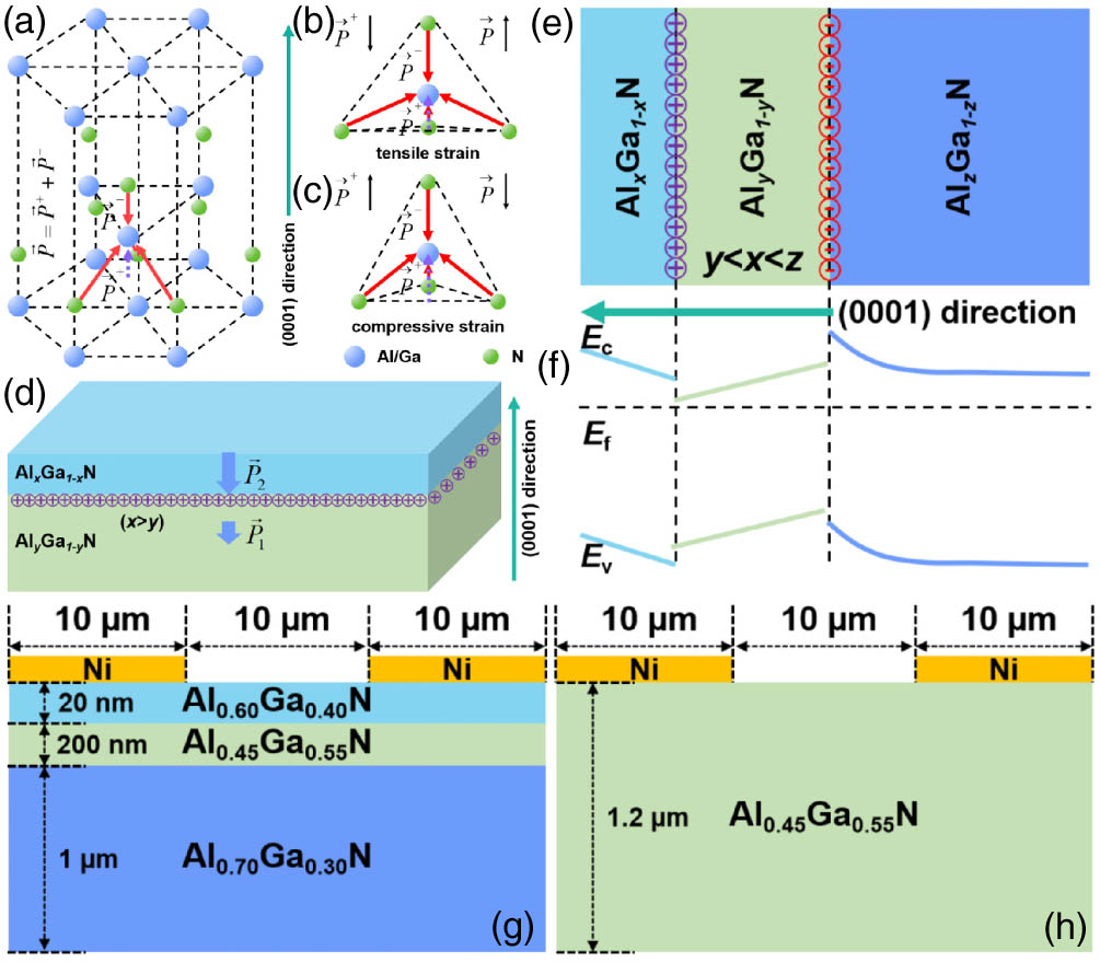
III-nitrides possess strong spontaneous and piezoelectric polarization [24,25]. The ionic bond component and the noncentrosymmetrical crystal structures result in spontaneous polarization [Fig. 1(a)]. The tensile or compressive strain can alter the bond angle and further result in piezoelectric polarization [Figs. 1(b) and 1(c)]. When the AlGaN materials form a heterostructure, the fixed charges will appear at the interface according to the Gauss law [Fig. 1(d)]. This is also the underlying mechanism that the high-concentration 2DEG can be formed at the interface. The polarization effect has significant impacts on the performance of III-nitrides-based devices. As for light-emitting diodes (LEDs), the polarization will separate the electrons and holes in the quantum wells and, thus, cause a sharp reduction of wave function overlap between the electron and hole (quantum-confined Stark effect, QCSE), which severely deteriorates the recombination of carriers [26]. Therefore, nonpolar III-nitrides are being developed to eliminate the polarization effect [27]. However, the polarization is not always harmful to devices. For example, the success of high electron mobility transistor (HEMT) strongly depends on the polarization-induced 2DEG [28]. Therefore, the role of the polarization effect in devices depends on the design. For AlGaN SBUV detectors, if the built-in field in the absorption layer can be enhanced by controlling the polarization [Figs. 1(e) and 1(f)], the photogenerated electron-hole pairs can be separated more efficiently and thus the carrier collection efficiency can be improved.
Sign up for Photonics Research TOC. Get the latest issue of Photonics Research delivered right to you!Sign up now
Figure 1.(a) Lattice diagram of hexagonal structure and origination scheme of polarization. (b), (c) Polarization variation under tensile and compressive strain. (d) Origination of interface charges due to polarization effect. (e), (f) Charge distribution and energy band diagram of AlGaN heterostructure. (g), (h) Designed devices and in simulations.
In this work, the polarization effect was utilized to improve the performance of AlGaN SBUV detectors. AlGaN heterostructures were designed to enhance the built-in field in the absorption layer. Two effects were generated: 1) the photogenerated electron-hole pairs were effectively separated, thus obtaining a longer carrier lifetime; 2) an ultrahigh electron mobility conduction channel was formed, thus achieving a faster electron transport speed. As a result, an SBUV detector with a high peak of 1.42 A/W at 10 V was achieved, being 50 times higher than the nonpolarization-enhanced one. It is worth mentioning that the polarization effect did not severely affect the response speed. Furthermore, a high work function metal (Ni/Au) was adopted as an electron reservoir to modify the polarization effect. A higher peak of 3.1 A/W at 30 V and a better signal-to-noise ratio (SNR) were finally realized. The investigation provided feasible approaches to improve the performance of AlGaN SBUV detectors by taking advantage of its inherent property.
2. MATERIALS AND METHODS
A. Simulations
Simulations were employed to predict the effects of polarization on the device performances. The polarization-enhanced detector in simulations is labeled as device [Fig. 1(g)]. For comparison, a nonpolarization-enhanced one was designed as device [Fig. 1(h)]. The Al content of the absorption layers was designed as 45%. The commercial APSYS software was used in simulations. The simulations were conducted by self-consistently solving the Poisson’s equation, continuity equation, and drift-diffusion equation with proper boundary conditions. Important factors include polarization level of 60%, defect-induced carrier lifetime of 3 ns [29], hole and electron mobility of 5 and [30,31], Schottky barrier heights of and contacts of 1.96 and 1.73 eV (Appendix A), and the energy band offset ratio for AlGaN heterojunction of 50:50 [32], respectively. The optical absorption coefficients for AlGaN layers were extracted from Refs. [33,34].
B. Materials Growth
The epilayers of devices and were grown on an AlN/sapphire template by high-temperature metal–organic chemical vapor deposition (HT-MOCVD). The trimethyl aluminum (TMAl), trimethyl gallium (TMGa), and ammonia () were used as the Al, Ga, and N precursors, and the hydrogen () was used as the carrier gas, respectively. An AlN epilayer was regrown on the AlN/sapphire template at 1300°C before AlGaN epilayers to improve the surface morphology. Then, AlGaN hetero-epilayers were grown on the as-grown AlN/sapphire template at 1180°C. Through tuning the Al/Ga source ratio, the designed Al content of each layer can be realized.
C. Device Fabrication
Standard photolithography processes and e-beam evaporation were adopted to fabricate the devices and . Interdigital grooves were first made on the photoresist mask by standard photolithography. 20/60 nm Ni/Au films were then deposited on the photolithograph-completed epitaxial wafers by e-beam evaporation. After lift-off process, the fabricated devices were rapidly annealed at 450°C for 3 min in atmosphere to make Schottky contact. Moreover, a device with an electron reservoir structure was fabricated, labeled as device . First, 20/60 nm Ti/Al electrodes were deposited, followed by annealing at 600°C for 30 s in atmosphere to form the source and drain. Then, semitransparent Ni/Au films (, Fig. 7 in Appendix A) were deposited between the source and drain as an electron reservoir, followed by annealing at 550°C for 5 min in atmosphere to form a higher Schottky barrier.
D. Characterizations
The in situ reflectance curves were used to monitor the epilayer growth rate. A high-resolution X-ray diffractometer (HRXRD, Bruck D8 discover) was adopted to estimate the Al content and crystal quality of the epilayers. An FL920 spectrophotometer was utilized to measure the absorption and transmission spectra of the as-grown epilayers. The IV curves were measured by a Keithley 6487. The spectral responses were measured by a DSR100 system with a xenon lamp, chopper, monochromator, Keithley 6487, SR830 lock-in amplifier, and standard Si detector. All response spectra were calibrated by the standard Si detector (Appendix A). The transient response spectra were measured by a RIGOL DS6104 digital oscilloscope. A pulse laser with emission wavelength of 266 nm, average power of 20 mW, repetition rate of 3 kHz, and pulse width of 10 ns was used to measure the photocurrent and transient responses.
3. RESULTS AND DISCUSSIONS
The energy band, electric field profile, and carrier distribution of devices and in dark and on illumination have been simulated to analyze the performance. The energy band of device in the equilibrium state bends heavily due to the polarization-effect-induced interface charges [upper panel in Fig. 2(a)]. The energy band of the absorption layer bends down toward the interface from the interface, which indicates there exists a strong built-in field in the absorption layer from the interface to the interface. The built-in field in the absorption layer in the equilibrium state is calculated to be as high as [Fig. 2(b)]. Such a high electric field can efficiently separate the electrons and holes to different areas. The holes and electrons separately accumulate at the and interfaces [Fig. 2(c)], confirming this conception. In this case, the electrons mainly contribute to the current, promising the fast response speed. When device is illuminated at 280 nm, the energy band bends less [lower panel in Fig. 2(a)]. It is because most of the photogenerated electron-hole pairs in the absorption layer are separated and swept toward the interface and interface, respectively, and the polarization-effect-induced interface charges are partially screened. Despite the screening effect, the built-in field still reaches as high as 0.1–0.2 MV/cm [Fig. 2(b)], guaranteeing the sustained photogenerated carriers’ separation ability when illuminated. As expected, the total carrier concentration becomes higher, and the electrical conducting layer extends deeper on illumination than in dark [Fig. 2(c)].
Figure 2.Simulated energy-band diagram, electric field, and carrier concentration in dark and on illumination for devices (a)–(c) and (d)–(f) , respectively.
For the nonpolarization-enhanced device , the energy band does not bend as severely as device [upper panel in Fig. 2(d)]. The slight band bending beneath the surface originates from the Schottky contact barrier in the simulation. Actually, the surface states can also cause such band bending in practical devices [35–38]. According to the band bending, it can be deduced that the built-in field points to the surface and that the value is much lower than that of device . The simulated average electric field within 200 nm beneath the surface is merely 0.02 MV/cm in dark [Fig. 2(e)], which is an order of magnitude smaller than that of device , indicating the weaker carriers’ separation ability of device . This is verified by the smaller concentration difference between the hole and electron around the surface of device [Fig. 2(f)]. In this case, both electrons and holes can contribute to the current. On illumination, the energy band bending becomes less, too [lower panel in Fig. 2(d)]. The average built-in field within 200 nm beneath the surface reduces to 0.01 MV/cm [Fig. 2(e)]. At such a low field, the photogenerated electron-hole pairs cannot be effectively separated [Fig. 2(f)]. The carrier lifetime will be shorter because of the huge overlap between electron and hole profiles and both types of carriers will contribute to the current, resulting in a poor and SNR. Hence, it can be predicted that the polarization effect can handle positive effects when improving AlGaN SBUV detector performance.
To confirm our above analyses, the current-voltage (IV) and response characters of devices and have been calculated. The dark current of device is several magnitudes lower than that of device , especially at low biases [Fig. 3(a)], which come from the higher Schottky barrier and the single type of carrier conduction of device . When illuminated at 280 nm, the currents sharply increase and reach a similar order of magnitude for both devices. However, the difference between the photocurrent and dark current of device is significantly higher than that of device [Fig. 3(a)]. It can result in higher and better SNR, which is proved by the simulated response spectra [Fig. 3(b)]. At biases from 5 to 20 V, the of device is always lower than that of device and so does the SBUV/VBUV ratio (). The performance variation trends of devices and demonstrate that the performance of the polarization-enhanced detector can surely exceed that of the nonpolarization-enhanced one.
Figure 3.Simulated (a) IV curves in dark and on illumination and (b) spectral responses under different biases for devices and (semilog scale in the inset).
Experiments have been performed to confirm the superiority of the polarization-enhanced detector over the nonpolarization-enhanced one. Epilayers of devices and are grown on an AlN/sapphire template [Fig. 4(a)]. According to the reflectance curves, the regrown AlN layer is about 500 nm for both epitaxial wafers, the , , and layers of device are about 1 μm, 200 nm, 20 nm, and the layer of device is about 1.2 μm, respectively, which satisfies the design requirements [Fig. 4(b)]. The HRXRD scanning of the epitaxial wafer for device exhibits three peaks near 36°, 35.5°, and 35.3°, which correspond to AlN, , and [39–43], respectively [upper panel in Fig. 4(c)]. The diffraction signal of 20 nm layer is too weak to be distinguished from the two peaks of and layers. The epitaxial wafer for device exhibits two HRXRD scanning peaks near 36° and 35.3°, corresponding to AlN and , respectively [lower panel in Fig. 4(c)]. The HRXRD results indicate the Al contents of the epitaxial wafers for devices and satisfy the design requirements. The full widths at half-maximum (FWHMs) of (0002) plane HRXRD rocking curve scanning (XRC) of the absorption layer of the epitaxial wafers for devices and are 379 and 418 arcsec, respectively, implying the similar crystal quality between devices and [Fig. 4(d)]. Absorption spectra of the epitaxial wafers for devices and show a 280 nm cutoff wavelength, ensuring the SBUV detection character [Fig. 4(e)]. The optical microscopy image illustrates the electrodes of the fabricated devices and . The length, width, and spacing of the interdigital electrodes of devices and are 190, 10, and 10 μm. The devices are front-illuminated when working [Fig. 4(f)]. The effective photosensitive area of devices and is the region between the two interdigital electrodes [Fig. 8(a) in Appendix A].
Figure 4.(a) Schematic epitaxial structures of devices and . (b) Temperature and reflectance curves during the growth procedure of devices and (inset). (c), (d) XRD and XRC results of the wafers for devices and . (e) Absorption spectra of the wafers for devices and . (f) Structure diagram and electrode optical image of the fabricated devices.
The IV curves of devices and in dark and on illumination have been measured. The difference between photocurrent and dark current of device is much larger than that of device [Fig. 5(a)], which coincides with our simulations, indicating the polarization-enhanced detector has better response, including and SNR, than the nonpolarization-enhanced one. However, at biases between , the dark current of device is higher than that of device , which deviates from the simulations [Figs. 5(a) and 3(a)]. It is likely because the interface-defect-induced tunneling current and surface-defect-induced surface current cannot be considered in the simulations, leading to the underestimation of dark current of device [Fig. 5(c)]. Meanwhile, since device has a traditional back-to-back Schottky-type MSM structure, the two Schottky junctions are always oppositely biased. At low biases, the forward-biased junction cannot be completely turned on, and there still exists a built-in field to suppress the thermal emission current. When the bias increases, the forward-biased junction is fully turned on, and the thermal emission current will remarkably increase [Fig. 5(b)]. The phenomena that the dark current of device keeps low within and rapidly rises with the increasing voltage, and that the photocurrent exhibits the same trend as the dark current, verify it [Fig. 5(a)].
Figure 5.(a) IV curves in dark and on illumination for devices and . (b), (c) Band diagrams of devices and in dark. (d) Spectral responses of devices and (inset). (e), (f) Band diagrams of devices and on illumination. (g) Response time of devices and as a function of load resistance. Inset: Normalized transient spectra at . (h) Schematic circuit to measure the transient spectra.
From the IV curves in dark, it can be deduced that the Schottky barrier of device is lower than that of device . On illumination, the current of device is lower than that of device within . The higher Schottky barrier of device should be responsible for it because the carriers cannot overcome the barrier at low voltage. The photocurrent of device exceeds that of device with the increasing bias because the applied voltage can overcome the higher Schottky barrier. The rapidly raising dark current made the photocurrent of device exceed that of device again, indicating that the SNR of device will become better than that of device with increasing bias [Fig. 5(a)].
The calibrated spectral response can more intuitively reflect the final device performance. Both devices produce a long-wavelength cutoff edge of 280 nm, demonstrating that the devices retain SBUV detection ability [Fig. 5(d)]. Device exhibits a peak response at around 257 nm. At biases of 5 V and 10 V, the can reach 1.18 A/W and 1.42 A/W with the SBUV/VBUV ratios of about 260 and 220. At even higher bias of 20 V, the can reach as high as 1.78 A/W, which is a competitive value even in real applications [Fig. 5(d)]. For comparison, device shows a peak response at around 255 nm. With the bias increasing from 5 V to 10 V, the rises from 0.022 A/W to 0.0285 A/W. The SBUV/VBUV ratios at 5 V and 10 V are about 90 and 60, respectively [inset of Fig. 5(d)]. These results obviously reflect that the polarization effect has enhanced the by about 50 times at the same bias and the SNR can also be improved. As shown, the results such as peak , peak wavelength, and SBUV/VBUV ratios of devices and are different from the simulated ones [Fig. 3(b)]. It is mainly because the optical absorption coefficients and light illumination power density of the practical devices are different from those used in the simulations.
For the traditional Schottky-type MSM detector, the applied electric field separates the photogenerated electron-hole pairs and drives the electrons and holes to move in opposite directions. In this case, the electrons and holes transport in the same areas, and the carrier lifetime will be shorter because they are easy to recombine [Fig. 5(e)]. Although both types of carriers can contribute to the photocurrent, the current gain (), which is determined by the carrier lifetime () and transit time (), can be very low (), resulting in a poor response [44,45]. Fortunately, the polarization effect brings about effective solutions. First, the polarization-induced 2DEG with ultrahigh electron mobility of over is the only conduction channel [Fig. 5(f), and Fig. 9 in Appendix A]. It can tremendously reduce the carrier transit time. Second, the polarization-enhanced built-in field in the absorption layer is vertical to the carrier transport channel. It separates the photogenerated electron-hole pairs and sweeps the electrons into the conduction channel and the holes to the opposite direction [Fig. 5(f)]. The inherent existence of the built-in field makes electrons of less possibility recombine with the hole and, hence, obtain a longer lifetime, leading to better response. Moreover, the strong polarization effect prevents the hole from contributing to the current, which is helpful in reducing noise. It is also a reason why device can exhibit higher SNR than device .
Because of the opposite carrier lifetime dependence of gain and carrier recombination time, there is usually an opposite trend between responsivity and response speed. Longer carrier lifetime usually leads to higher responsivity and slower response speed due to the higher gain and longer carrier recombination process. To value the effect of the polarization on response time, the transient response spectra at different load resistances have been measured. The detector is connected to an adjustable load resistance and inserts into a circuit with sustainable and stable terminal voltage of 8 V. The pulse laser directly illuminates on the detector, and the oscilloscope simultaneously measures the voltage variation of the load resistance [Fig. 5(h)]. The response times are extracted by exponentially fitting the transient response spectra [inset of Fig. 5(g)]. Since the polarization-effect-enhanced built-in field prolongs the carrier lifetime, it can be speculated that device will have slower response speed than device . The response time at load resistance from to has been measured for devices and [Fig. 5(g)]. It can be seen that the response time of device is always smaller than that of device , confirming the polarization effect. We have extrapolated the response time at zero load resistance according to the response time variation trends. The extrapolated response times of devices and are 7.6 and 3.5 μs, respectively, which can be considered as their inherent response times. Although the response speed of device has been slowed down compared with device , it still maintains a relatively high response speed due to the short transient time.
It has been verified that the enhanced polarization effect can improve the detector performance above. However, it is also noted that the dark current level is not low enough because of the high concentration 2DEG. Besides, the polarization-induced 2DEG will conversely screen the polarization-induced built-in field, lowering the separation efficiency of photogenerated electron-hole pairs. Therefore, if the 2DEG concentration can be effectively controlled, the device performance such as and SNR ought to be further improved. As is known, metals can usually act as electron reservoirs to provide or store electrons. By contacting a high work function metal to a semiconductor, the electrons can transport to the metal through tunneling or thermal emission if the metal work function is higher than that of the semiconductor [Fig. 6(a)]. Therefore, we employ a structure in which a metal electron reservoir is deposited between the source and drain electrodes (). The optical microscopy image illustrates the electrodes and metal electron reservoir of device . The spacing between the source and drain electrodes is 20 μm, and the source and drain electrode widths are both 100 μm. The electron reservoir locates at the center between the source and drain and the width is 10 μm. Device is also front-illuminated when working [Fig. 6(b)]. The effective photosensitive area is estimated to be 80% of the area between the source and drain electrodes due to the semitransparent electron reservoir structure [Fig. 8(b) in Appendix A].
Figure 6.(a) Band alignment and carrier distribution with high work function metal to adjust the carrier concentration. (b) Structure diagram and electrode optical image of device . (c) IV curves of device in dark and on illumination. (d) Spectral response of device under different biases.
The IV curves of device have been measured in dark and on illumination to investigate the device performance [Fig. 6(c)]. Apparently, the difference between the photocurrent and dark current of device is further increased compared with devices and . It is found that the dark current is reduced by over three orders of magnitude at the same biases. Considering the effective area difference among the devices, it can be deduced that the dark current density of device has been decreased by at least one order of magnitude. Besides, the photocurrent reaches about 10 μA, which is the same magnitude as that of devices and . Taking the effective device area into consideration, we can also speculate that the collection efficiency of the photogenerated carriers has been improved. Spectral responses at different biases have been measured to examine the performance [Fig. 6(d)]. The cutoff wavelength still locates at around 280 nm. At biases of 5, 10, and 20 V, the peak R are 1.75, 2.31, and 2.51 A/W, respectively, which are remarkably higher than the values of device at the same biases. By further elevating the bias to 30 V, the peak can reach as high as 3.1 A/W, thus demonstrating the excellent performance of device . Besides, the SBUV/VBUV ratios of device at different biases are calculated to be over , which is much higher than that of devices and , also indicating the better performance of device .
4. CONCLUSIONS
In summary, AlGaN SBUV detectors were fabricated and investigated. The inherent polarization effect was utilized to improve the device performance. AlGaN heterostructures were designed to modify the polarization effect and to enhance the built-in field in the absorption layer. The polarization-enhanced detector realized a 50 times improvement on the peak compared with the nonpolarization-enhanced one. A peak of 1.16 A/W at 5 V and a better SNR were achieved. The longer carrier lifetime at the absorption layer and the ultrahigh electron mobility conduction channel induced by the polarization effect were responsible for the improvements. Elimination of the hole current also partially contributed to the improvements. Besides, the polarization effect did not severely postpone the response speed due to the fast carrier drift speed in the conduction channel. Furthermore, an electron reservoir structure was proposed to improve the response character. A higher peak of 3.1 A/W at 30 V and a better SNR were achieved since the electron reservoir structure could modulate the polarization-induced 2DEG concentration in the conduction channel to suppress the dark current and enhance the separation efficiency of photogenerated electron-hole pairs. We believe that the investigations here provide alternative and feasible approaches for the community to improve the AlGaN SBUV detector performance.
APPENDIX A
Determination of Schottky Barrier Height in Simulations
The APSYS software will calculate the Schottky barrier height between metals and AlGaN materials by considering the work function of the metal, the electron affinity of the AlGaN material, the image force, the applied bias, etc. Generally, the work function of a metal can be easily found. In our simulations, we set the work function of Ni as 5.15?eV [46–49]. Simultaneously, the APSYS software will determine the electron affinity of according to the Al content of . In our simulations, we set the of layer contacted to the Ni electrodes as 0.60 and 0.45 for devices and , respectively, as designed. By self-consistently considering the metal work function, semiconductor electron affinity, image force, applied bias, etc., the APSYS software finally gave the Schottky barrier heights of the and contacts of 1.96 and 1.73?eV, respectively.
Transmittance Spectrum of the Ni/Au Semitransparent Film
To ensure the semitransparent characterization of the Ni/Au film deposited on the device as the electron reservoir structure, we measured the transmittance spectrum of the Ni/Au film deposited on a sapphire substrate by the same conditions and parameters as the Ni/Au film on device . The experiment was carried out on an FL920 spectrophotometer, and the sapphire substrate was used to subtract the background. Figure?7 shows the transmittance spectrum of the Ni/Au semitransparent film from 200 to 700?nm. As shown, the transmittance of the as-deposited Ni/Au film is near 60% in the solar-blind wavelength range.
Figure 7.Transmittance spectrum of the Ni/Au semitransparent film.
Figure 9.(a) measurement results of the wafer for devices and . (b) Ohmic check for Hall measurements at room temperature. (c) Temperature-dependent Hall measurement results of the wafer for devices and .
Temperature-dependent Hall measurement by van der Pauw method was performed at temperatures from 50 to 310?K and magnetic field of 9?kG with a wafer cut of . Since the wafer was not capped by a GaN contact layer, it was difficult to directly form ohmic contact to the upper layer; further, the contact resistance was too high to perform the measurement. Hence, we etched about 60?nm at the four corners of the cut by an inductively coupled plasma system (ICP, Oxford Plasmalab System 100), so that the metal electrodes can effectively contact the 2DEG. Figure?9(b) shows the ohmic check results among the four electrodes at room temperature. It is shown that all electrodes are ohmic contacts, guaranteeing the correctness of the Hall measurement. Figure?9(c) shows the temperature-dependent electron mobility (upper), electron sheet concentration (middle), and sheet resistance (lower). As temperature increases from 50 to 310?K, the electron sheet concentration almost keeps constant, which again demonstrates that the 2DEG induced by polarization effect is the main conduction channel. The electron sheet concentration is about , which coincides well with the result because the 2DEG is always confined within several nanometers at the interface. As for the electron mobility, it first increases and then decreases with temperature increasing. This is because the impurity scattering effect gradually decreases and the phonon scattering effect simultaneously increases with the temperature ramping. Although the 2DEG mobility decreases with temperature rising, it is still higher than at 300?K, which is much higher than that of the electrons in single-layer AlGaN film. Since the electron sheet concentration keeps almost constant, the sheet resistance is generally determined by the mobility.