• Photonics Research
  • Vol. 11, Issue 7, 1154 (2023)
Zhibiao Zhu1、†, Zhe Qin1、†, He Wang1, Lixin Jiang1, Yongfeng Li1、*, Wenjie Wang1, Hongya Chen1, Jiafu Wang1, Yongqiang Pang2, and Shaobo Qu1
Author Affiliations
  • 1Shaanxi Key Laboratory of Artificially-Structured Functional Materials and Devices, Air Force Engineering University, Xi’an 710051, China
  • 2School of Electronic Science and Engineering, Xi’an Jiaotong University, Xi’an 710049, China
  • show less
    DOI: 10.1364/PRJ.468496 Cite this Article Set citation alerts
    Zhibiao Zhu, Zhe Qin, He Wang, Lixin Jiang, Yongfeng Li, Wenjie Wang, Hongya Chen, Jiafu Wang, Yongqiang Pang, Shaobo Qu. Switchable chiral mirror based on PIN diodes[J]. Photonics Research, 2023, 11(7): 1154 Copy Citation Text show less
    (a) Conventional mirror (metallic plate) reverses the handedness of incident CP waves. Here, we report switchable chiral mirrors that transform upon regulating voltage into (b) a handedness-preserving mirror, (c) a perfect absorber, and (d) an LCP/(e) an RCP mirror. Handedness-preserving mirrors reflect both CP waves without handedness change. In addition, the LCP/RCP mirror reflects the LCP/RCP wave without handedness reversal while absorbing the other CP waves. Moreover, the perfect absorber absorbs both LCP and RCP waves.
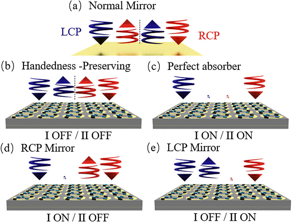
    Fig. 1. (a) Conventional mirror (metallic plate) reverses the handedness of incident CP waves. Here, we report switchable chiral mirrors that transform upon regulating voltage into (b) a handedness-preserving mirror, (c) a perfect absorber, and (d) an LCP/(e) an RCP mirror. Handedness-preserving mirrors reflect both CP waves without handedness change. In addition, the LCP/RCP mirror reflects the LCP/RCP wave without handedness reversal while absorbing the other CP waves. Moreover, the perfect absorber absorbs both LCP and RCP waves.
    Schematic diagram of the unit cell of the switchable chiral mirror. (a) The perspective view and (b) the front view of the structure. (c) PIN diode equivalent circuit. (d) View of the Via design. Vias I and II have no contact with the intermediate metal layer, and Via III is connected to the middle metal layer. (e) The front view of the middle metallic layer. (f) The bottom feeder design. The two thin metal wires are connected to separate electrodes, respectively.
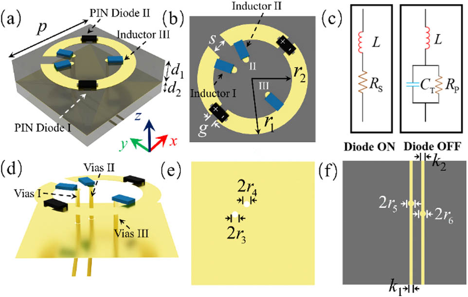
    Fig. 2. Schematic diagram of the unit cell of the switchable chiral mirror. (a) The perspective view and (b) the front view of the structure. (c) PIN diode equivalent circuit. (d) View of the Via design. Vias I and II have no contact with the intermediate metal layer, and Via III is connected to the middle metal layer. (e) The front view of the middle metallic layer. (f) The bottom feeder design. The two thin metal wires are connected to separate electrodes, respectively.
    Simulated (a) absorption spectra, (b) reflection amplitudes (|r|), and (c) CD spectra of the handedness preserving mirror state (PIN diode I OFF, PIN diode II OFF) at normal incidence. Simulated (d) absorption spectra, (e) reflection amplitudes, and (f) CD spectra of the perfect absorber state (PIN diode I ON, PIN diode II ON) at normal incidence. Simulated (g) absorption spectra, (h) reflection amplitudes, and (i) CD spectra of the RCP mirror state (PIN diode I ON, PIN diode II OFF) at normal incidence. Simulated (j) absorption spectra, (k) reflection amplitudes, and (l) CD spectra of the LCP mirror state (PIN diode I OFF, PIN diode II ON) at normal incidence.
    Fig. 3. Simulated (a) absorption spectra, (b) reflection amplitudes (|r|), and (c) CD spectra of the handedness preserving mirror state (PIN diode I OFF, PIN diode II OFF) at normal incidence. Simulated (d) absorption spectra, (e) reflection amplitudes, and (f) CD spectra of the perfect absorber state (PIN diode I ON, PIN diode II ON) at normal incidence. Simulated (g) absorption spectra, (h) reflection amplitudes, and (i) CD spectra of the RCP mirror state (PIN diode I ON, PIN diode II OFF) at normal incidence. Simulated (j) absorption spectra, (k) reflection amplitudes, and (l) CD spectra of the LCP mirror state (PIN diode I OFF, PIN diode II ON) at normal incidence.
    The surface current distributions of the switchable chiral mirror at the handedness preserving mirror state under the normal incidence of (a) LCP and (b) RCP waves at 13 GHz, respectively. The surface current distributions of the switchable chiral mirror at the absorber state under the normal incidence of (c) LCP and (d) RCP waves at 13 GHz, respectively. The surface current distributions of the switchable chiral mirror at the RCP mirror state under the normal incidence of (e) LCP and (f) RCP waves at 13 GHz, respectively. The surface current distributions of the switchable chiral mirror at the LCP mirror state under the normal incidence of (g) LCP and (h) RCP waves at 13 GHz, respectively. Arrows indicate electric dipoles corresponding to resonant currents excited by the CP waves of opposite handedness.
    Fig. 4. The surface current distributions of the switchable chiral mirror at the handedness preserving mirror state under the normal incidence of (a) LCP and (b) RCP waves at 13 GHz, respectively. The surface current distributions of the switchable chiral mirror at the absorber state under the normal incidence of (c) LCP and (d) RCP waves at 13 GHz, respectively. The surface current distributions of the switchable chiral mirror at the RCP mirror state under the normal incidence of (e) LCP and (f) RCP waves at 13 GHz, respectively. The surface current distributions of the switchable chiral mirror at the LCP mirror state under the normal incidence of (g) LCP and (h) RCP waves at 13 GHz, respectively. Arrows indicate electric dipoles corresponding to resonant currents excited by the CP waves of opposite handedness.
    The energy loss distributions on the structure surface at the handedness preserving mirror state under the normal incidence of (a) LCP and (b) RCP waves at 13 GHz, respectively. The energy loss distributions on the structure surface at the absorber state under the normal incidence of (c) LCP and (d) RCP waves at 13 GHz, respectively. The energy loss distributions on the structure surface at the RCP mirror state under the normal incidence of (e) LCP and (f) RCP waves at 13 GHz, respectively. The energy loss distributions on the structure surface at the LCP mirror state under the normal incidence of (g) LCP and (h) RCP waves at 13 GHz, respectively.
    Fig. 5. The energy loss distributions on the structure surface at the handedness preserving mirror state under the normal incidence of (a) LCP and (b) RCP waves at 13 GHz, respectively. The energy loss distributions on the structure surface at the absorber state under the normal incidence of (c) LCP and (d) RCP waves at 13 GHz, respectively. The energy loss distributions on the structure surface at the RCP mirror state under the normal incidence of (e) LCP and (f) RCP waves at 13 GHz, respectively. The energy loss distributions on the structure surface at the LCP mirror state under the normal incidence of (g) LCP and (h) RCP waves at 13 GHz, respectively.
    Measured (a) absorption spectra, (b) reflection amplitudes, and (c) CD spectra of the handedness preserving mirror state at normal incidence. Measured (d) absorption spectra, (e) reflection amplitudes, and (f) CD spectra of the perfect absorber state at normal incidence. Measured (g) absorption spectra, (h) reflection amplitudes, and (i) CD spectra of the RCP mirror state at normal incidence. Measured (j) absorption spectra, (k) reflection amplitudes, and (l) CD spectra of the LCP mirror state at normal incidence.
    Fig. 6. Measured (a) absorption spectra, (b) reflection amplitudes, and (c) CD spectra of the handedness preserving mirror state at normal incidence. Measured (d) absorption spectra, (e) reflection amplitudes, and (f) CD spectra of the perfect absorber state at normal incidence. Measured (g) absorption spectra, (h) reflection amplitudes, and (i) CD spectra of the RCP mirror state at normal incidence. Measured (j) absorption spectra, (k) reflection amplitudes, and (l) CD spectra of the LCP mirror state at normal incidence.
    Photograph of the switchable chiral mirror prototype. (a) The measurement system, (b) the front view, and (c) the back view. All Vias I in a row are connected in a series on the backside of the dielectric substrate and connected to the top metal patch (not connected to the bottom metal patch). Feeder I provides voltage V1. All Vias II in a row are connected in a series on the backside of the dielectric substrate to connect to the bottom metal patch (without connecting to the top metal patch). Feeder II provides voltage V2. A separate Via in the lower right corner connects to the ground Via feeder III. It is worth noting that the metal backplane is in the middle layer, connected to feeder III through the Via in the lower right corner. (d) The local view.
    Fig. 7. Photograph of the switchable chiral mirror prototype. (a) The measurement system, (b) the front view, and (c) the back view. All Vias I in a row are connected in a series on the backside of the dielectric substrate and connected to the top metal patch (not connected to the bottom metal patch). Feeder I provides voltage V1. All Vias II in a row are connected in a series on the backside of the dielectric substrate to connect to the bottom metal patch (without connecting to the top metal patch). Feeder II provides voltage V2. A separate Via in the lower right corner connects to the ground Via feeder III. It is worth noting that the metal backplane is in the middle layer, connected to feeder III through the Via in the lower right corner. (d) The local view.
    Zhibiao Zhu, Zhe Qin, He Wang, Lixin Jiang, Yongfeng Li, Wenjie Wang, Hongya Chen, Jiafu Wang, Yongqiang Pang, Shaobo Qu. Switchable chiral mirror based on PIN diodes[J]. Photonics Research, 2023, 11(7): 1154
    Download Citation