
Zhibiao Zhu, Zhe Qin, He Wang, Lixin Jiang, Yongfeng Li, Wenjie Wang, Hongya Chen, Jiafu Wang, Yongqiang Pang, Shaobo Qu. Switchable chiral mirror based on PIN diodes[J]. Photonics Research, 2023, 11(7): 1154
- Photonics Research
- Vol. 11, Issue 7, 1154 (2023)
Abstract
1. INTRODUCTION
Chirality exists in natural structures and molecules, such as shells with mirror-image symmetry, DNA double helix structures, and amino acid molecules [1]. The three-dimensional (3D) chirality displayed by these biological structures is relatively weak and a challenge to improve, so applying it to practical applications is not easy. The emergence of chiral metamaterials can improve the chiral characteristics and electromagnetic (EM) response properties so that they can be used in different fields, and it can control the physical parameters of metamaterials to obtain responses in different frequency spectra [2–4]. The research on chiral metamaterials has been a significant research hotspot in the field of metamaterials, and it has unique EM and optical properties, such as asymmetric transmission [3,4], polarization conversion [5–7], circular dichroism (CD) [8,9], and chiral negative refractive index [10,11]. Meta-devices such as circular polarizers [12], broadband circular polarization converters [13], energy harvesters [14], and focusing lenses [15] have been realized.
Compared with the 3D chiral metamaterials, the planar two-dimensional (2D) chiral metamaterials have twisting characteristics, and when viewed from the opposite direction, the chirality of the 2D chiral metamaterials is precisely the opposite. Like the Archimedes spiral drawn on a transparent substrate, the spiral is reversed when viewed from the other side of the substrate. When planar metamaterials are under the illumination of the EM waves, whether the transmission or scattering effects depend on the twisted structure has attracted attention. Researchers have theoretically proved that planar metamaterials with this twisted structure can manipulate EM waves uniquely [16,17]. In addition, the planar structure has appeared one after another from the Greek cross fractal resonator [18], split-ring resonator [19], N-shaped resonator [20], Hilbert-shaped resonator [21], L-shaped resonator [22] to the fish-scale grid [23]. It further confirms experimentally that 2D chiral metamaterials have different rotations for left-handed circularly polarized (LCP) and right-handed circularly polarized (RCP) waves.
In recent years, chiral mirrors have been proposed to control CD, which is the differential reflection of LCP and RCP waves. Many novel designs that enhance CD have been reported and experimentally verified in the microwave and near-infrared regions. The 3D helical structure has strong inherent chirality and dipole–dipole interaction, producing large CD [24–27]. A multilayer chiral structure can create a more significant CD effect due to the interaction between layers [28,29]. In addition, a more extensive CD can be produced if a subwavelength chiral structure destroys both -fold rotational () symmetry and mirror symmetry [8]. After introducing resistance, the chiral mirror working in the microwave band can produce CD over broadband [30]. However, most chiral mirrors have fixed functions and can only absorb specific circularly polarized (CP) waves.
Sign up for Photonics Research TOC. Get the latest issue of Photonics Research delivered right to you!Sign up now
In this paper, we have experimentally proved that a switchable chiral mirror can be switched in four working states. As shown in Fig. 1, by independently controlling the ON and OFF of the two PIN diodes, we realize the electrical switching among the handedness-preserving mirror, perfect absorber, LCP mirror, and RCP mirror. Unlike using the asymmetry of the metallic pattern to achieve circular dichroism, we change the ON–OFF state of the PIN diodes to achieve distinct responses to two CP waves. When RCP and LCP waves are irradiated, stronger surface currents appear at different positions of the structure. The position of the PIN diode is determined according to this phenomenon. A switchable chiral mirror was manufactured based on the existing printed circuit board (PCB) technology, and experiments at microwave frequencies verified it. The thickness of the chiral mirror proposed in this paper is only one-tenth of the wavelength, conducive to chip integration. Such a switchable chiral mirror is highly versatile and can be applied in communications, information processing, imaging, and polarization-sensitive detection of EM waves.
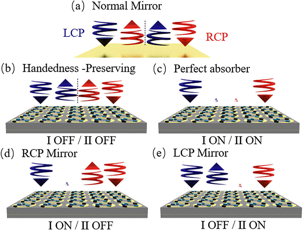
Figure 1.(a) Conventional mirror (metallic plate) reverses the handedness of incident CP waves. Here, we report switchable chiral mirrors that transform upon regulating voltage into (b) a handedness-preserving mirror, (c) a perfect absorber, and (d) an LCP/(e) an RCP mirror. Handedness-preserving mirrors reflect both CP waves without handedness change. In addition, the LCP/RCP mirror reflects the LCP/RCP wave without handedness reversal while absorbing the other CP waves. Moreover, the perfect absorber absorbs both LCP and RCP waves.
The schematic diagram of the switchable chiral mirror is shown in Fig. 2. For most chiral subwavelength structures, the key to achieving circular dichroism is that the structure should simultaneously destroy -fold () rotational symmetry and mirror symmetry. Based on this principle, a split-ring resonator is proposed as a proof-of-concept to support our design. After introducing resistance on the half-arm of the metallic pattern, the symmetry of its response to EM waves can be changed through ohmic loss [30]. Reference [30] points out that the strong surface currents appear at different locations when irradiated by LCP and RCP waves. Under LCP wave illumination, the strong surface current appears on the left arm of the split ring. After introducing a resistor on the left arm of the structure, the structure can realize the strong absorption of the LCP wave, while the RCP wave is almost completely reflected. The case of RCP wave incidence is similar. The strong surface current appears on the right arm of the split ring. Thus, the split ring loaded with resistance can realize circular dichroism. Two PIN diodes are loaded on the two arms of the split-ring resonator, and the switchable chiral mirrors can be realized through the ON–OFF switching of the PIN diodes. The unit cell of the switchable chiral mirrors is analyzed and optimized by the EM simulation software CST MICROWAVE STUDIO. The optimized parameters are as follows: , , , , , , and , as shown in Figs. 2(a) and 2(b). The switchable chiral mirror includes an upper FR4 substrate (relative dielectric constant of 4.4, loss tangent of 0.02), an intermediate metallic layer, a lower FR4 substrate, and a metallic pattern layer covering FR4. The middle homogeneous metallic layer realizes zero transmission.
![]()
Figure 2.Schematic diagram of the unit cell of the switchable chiral mirror. (a) The perspective view and (b) the front view of the structure. (c) PIN diode equivalent circuit. (d) View of the Via design. Vias I and II have no contact with the intermediate metal layer, and Via III is connected to the middle metal layer. (e) The front view of the middle metallic layer. (f) The bottom feeder design. The two thin metal wires are connected to separate electrodes, respectively.
As shown in Fig. 2(b), the anodes of PIN diodes I and II are on the upper side of the metallic split ring. A circuit in which the states of two PIN diodes can be independently controlled is designed. Via hole III is connected to the middle metallic layer as an electrode, and its top surface is connected to the lower end of the metallic split ring through Inductor III. Vias I and II connect the left and right sides of the opening of the metallic ring through an inductor, respectively. Vias I and II are connected to the feed lines at the bottom layer, each to a separate electrode. Figure 2(d) illustrates where Vias I and II do not directly contact the intermediate metal layer. The diameter of the copper column is 0.15 mm, , and , as illustrated in Figs. 2(e) and 2(f). The design of the round metallic gasket is to meet the needs of prototype processing and facilitate diode welding.
A suitable PIN diode (BAP70-02, NXP, Holland) [31] is selected according to the size of the switchable chiral mirror and the resistance value required to achieve the maximum CD. The PIN diode can be equivalent to a series connection of a small inductance () and forward resistance () in the ON state. The PIN diode can be equivalent to the parallel connection of reverse resistance () and equivalent capacitance () in the OFF state. The small series inductance also needs to be considered in the OFF state. In one unit cell, the value of the three-chip inductors is 27 nH, and they are welded between the direct current (DC) power lines and metallic pattern as a radio frequency choke. The inductors block alternating current but allow direct current paths.
2. SIMULATION RESULTS AND ANALYSIS
The complex Jones matrix describes the incidence and reflection of electromagnetic (EM) waves passing through the metasurface. The thickness of the metasurface is much smaller than the wavelength, which can be ignored in theoretical analysis. When LCP or RCP is vertically incident, the complex amplitudes of the circular polarization incident field and reflection field can be represented by the complex Jones matrix [32]:
For the reflection-type metasurface proposed in this paper, the CD spectrum can characterize the chirality of the structure, which describes the discrepancy between two CP waves in reflection (or absorption). The difference in reflection intensity for RCP and LCP illumination is
can then be obtained by changing the linear-polarization bases to the circular-polarization base with the following transformation: ,
A. Handedness Preserving Mirror State
The mirror that maintains handedness for the incident CP waves with either handedness shows the same anisotropic response. Therefore, when the switchable chiral mirror is in a mirror state that maintains handedness, the structure needs to keep anisotropy. When the two PIN diodes are both in the OFF state, the chiral EM response disappears. The switchable chiral mirror becomes a handedness-preserving mirror at the working frequency (13 GHz). Figures 3(a) and 3(b) show the spectral dependence of the switchable mirror’s absorption and reflectivity according to simulations when the working state is switched to the handedness preserving mirror state ( dominates, still exists but can be ignored). The reflection matrix for circular polarization is governed by eigenvectors and . At the handedness preserving mirror state, the reflection coefficients must satisfy , . According to Eq. (6), the solution can be obtained with . The eigenvalues of with the eigenvectors of and is obtained from the , which indicates that total reflections of LCP and RCP waves is achieved.
![]()
Figure 3.Simulated (a) absorption spectra, (b) reflection amplitudes (
Our simulation reveals the physical origin of the chirality-maintaining mirror state, which shows how the incident LCP and RCP interact with a split resonant ring loaded with two PIN diodes at 13 GHz. The current distribution on the metallic pattern surface has been studied and shown in Figs. 4(a) and 4(b). The redder the arrow color, the stronger the surface current. The surface currents induced on the metallic surface are weak under the irradiation of the LCP and the RCP waves. At this working state, the energy loss distributions of the structure show the same results, as shown in Figs. 5(a) and 5(b). The directions of the electric dipoles excited by the RCP and LCP waves are the same. The electric dipole effectively radiates, causing near-complete circular conversion ( and , respectively) and generating a counter-rotating field that is different from the incident CP wave. It is worth mentioning that the two PIN diodes are both in the OFF state, and the energy of the incident EM wave is almost not lost. At the handedness preserving mirror state, the value of the CD is zero at the working frequency band [as shown in Fig. 3(c)].
![]()
Figure 4.The surface current distributions of the switchable chiral mirror at the handedness preserving mirror state under the normal incidence of (a) LCP and (b) RCP waves at 13 GHz, respectively. The surface current distributions of the switchable chiral mirror at the absorber state under the normal incidence of (c) LCP and (d) RCP waves at 13 GHz, respectively. The surface current distributions of the switchable chiral mirror at the RCP mirror state under the normal incidence of (e) LCP and (f) RCP waves at 13 GHz, respectively. The surface current distributions of the switchable chiral mirror at the LCP mirror state under the normal incidence of (g) LCP and (h) RCP waves at 13 GHz, respectively. Arrows indicate electric dipoles corresponding to resonant currents excited by the CP waves of opposite handedness.
![]()
Figure 5.The energy loss distributions on the structure surface at the handedness preserving mirror state under the normal incidence of (a) LCP and (b) RCP waves at 13 GHz, respectively. The energy loss distributions on the structure surface at the absorber state under the normal incidence of (c) LCP and (d) RCP waves at 13 GHz, respectively. The energy loss distributions on the structure surface at the RCP mirror state under the normal incidence of (e) LCP and (f) RCP waves at 13 GHz, respectively. The energy loss distributions on the structure surface at the LCP mirror state under the normal incidence of (g) LCP and (h) RCP waves at 13 GHz, respectively.
B. Perfect Absorber State
When both PIN diodes are conducting, the switchable chiral mirror can be switched to the absorber state. At 13 GHz, the absorption rate of the absorber is above 90%. Both LCP and RCP waves are almost fully absorbed at their working frequency band through the ohmic loss of two PIN diodes. Figures 3(d) and 3(e) show the simulated absorption and reflectivity of the absorber when PIN diodes I and II are in the ON state. At the absorber state, the reflection coefficients must satisfy . According to Eq. (6), the solution can be obtained with . The eigenvalues of with the eigenvectors of and are obtained from the , which indicates that total absorption of the LCP and the RCP waves is achieved.
Our simulation reveals the physical origin of the absorber state, which shows how the incident LCP and RCP interact with the split resonant ring loaded with two PIN diodes at 13 GHz. In this working state, the current on the surface of the metallic pattern is stronger under the incidence of two CP waves. Figures 4(c) and 4(d) show the instantaneous distribution of the surface current. In fact, we observed in the animation of surface current that a strong surface current oscillates back and forth on the left arm of the split ring under LCP wave irradiation. The LCP wave excites strong electric dipole. The strong currents just go through the PIN diode on the left arm. The diode is in a conducting state (), resulting in a large loss of EM waves. Notably, the current on the right arm is weak under LCP illumination. Under the irradiation of the RCP wave, a strong current oscillates back and forth on the right arm of the split ring, and the analysis is similar to that of the LCP wave. As a verification, the energy loss distributions are provided in Figs. 5(c) and 5(d), which show that under the incidence of the LCP and the RCP waves, the location where the loss occurs is different. At the perfect absorber state, the value of the CD is zero at the working frequency band [as shown in Fig. 3(f)].
C. RCP Mirror State
The split-ring resonator proposed in this paper is loaded with PIN diodes to change the symmetry of the structure’s response to two CP waves. When PIN diode I is in the ON state and PIN diode II is in the OFF state, the state of the chiral mirror is switched to the RCP mirror. At its resonance (), the RCP wave intensity is almost fully reflected without handedness change (), while the LCP wave is almost fully absorbed through the ohmic loss of PIN diode I. Figures 3(g) and 3(h) show the simulated structure’s absorption and reflectivity at the RCP mirror state. At the RCP mirror state, the reflection coefficients must satisfy , . According to Eq. (6), the solution can be obtained with . The eigenvalue of with the eigenvector of indicates that total absorption of LCP is achieved, and the eigenvalue of with the eigenvector of indicates that total reflection of RCP is achieved.
Our simulation reveals the physical mechanism behind the RCP mirror. The distribution of the surface current and the energy loss can directly analyze the cause of the CD generation of the switchable chiral mirror at the RCP mirror state. The RCP mirror response is caused by the two linear electric dipoles excited by LCP and RCP [Figs. 4(e) and 4(f)]. Under the irradiation of the LCP wave, strong surface currents oscillate back and forth on the left arm of the split ring and form a strong electric dipole. The PIN diode on the left arm is ON (), which results in a large loss of the LCP wave. Meanwhile, the surface current on the right arm of the split ring is weak, forming a weak electric dipole. The PIN diode of the right arm is in the OFF state, so the RCP wave is almost not lost. The distribution of energy loss in the RCP mirror state verifies the above derivation [as shown in Figs. 5(e) and 5(f)]. The different energy losses result in the absorption of the structure under the LCP wave incidence being larger than that under the RCP wave. At the RCP mirror state, the sign of the CD is negative at the working frequency band [as shown in Fig. 3(i)].
It is necessary to explain why the electric dipole mode can cause a nearly perfect reflection of the RCP. The ideal linear electric dipole radiates linear polarization, that is, the superposition of equal-strength fields with opposite handedness. The fields radiated along and rotating together with the incident field can (destructively) interfere with the incident field (along ) and with its reflection by the metal backing plate (along ). In this way, the field rotating in the same direction as the incident disappears in the structure at the RCP mirror state. The radiation field rotating in the opposite direction compared with the incident field still exists (circular polarization conversion). These counter-rotating incident and reflected fields have the same circular polarization when propagating in the opposite direction, which means that their handedness must be evaluated by an observer looking from the opposite direction.
D. LCP Mirror State
In order to realize a chiral mirror with opposite handedness, a diode configuration with opposite circular conversion dichroism is required. Therefore, compared to the RCP mirror, it is necessary to reverse the ON–OFF configuration of the two PIN diodes to convert the chiral mirror to the opposite handedness. When the diode loaded on the left arm is in the OFF state, and the diode on the right arm is in the ON state, the state of the chiral mirror is switched to the RCP mirror state. At its resonance (), the LCP intensity is almost fully reflected without a chiral change (), while RCP is almost fully absorbed through the ohmic loss of PIN diode II [Figs. 3(j) and 3(k)]. This phenomenon corresponds to a nearly perfect CD conversion, where is almost unity. At the LCP mirror state, the reflection coefficients must satisfy , . According to Eq. (6), the solution can be obtained with . The eigenvalue of with the eigenvector of indicates that total absorption of RCP is achieved. The eigenvalue of with the eigenvector of indicates that total reflection of LCP is achieved.
The physical origin of the LCP mirror is revealed by simulating the excitation mode of the incident LCP and RCP through the chiral resonance of the structure. This part of the analysis is the same as the RCP mirror. The electric dipole excitation is induced by LCP [Fig. 4(g)], which leads to a nearly complete circular conversion (). Under RCP wave illumination, strong surface currents oscillate back and forth on the right arm of the split ring, and a strong electric dipole is excited [Fig. 4(h)]. The PIN diode on the right arm is ON (), and a strong surface current passes through the diode, resulting in complete absorption of the RCP wave. In the working state of the LCP mirror, the value of the CD is positive.
3. EXPERIMENTAL RESULTS
Figure 6 shows experimental results, which are in good agreement with the simulation results. As shown in Fig. 7, a prototype of the switchable chiral mirror was manufactured and measured to verify the simulation. The prototype includes unit cells arranged in the same direction with a total area of , and four DC power lines are etched on the four sides of the panel. Two BAP 70-02 PIN diodes and three 27 nH chip inductors with a package of are soldered on each unit cell. According to the datasheet of the diode, the operating power range of the PIN diode is 0–0.02 W. The voltages on the periphery of the prototype are and , which control the states of all PIN diodes I and II, respectively. and are provided by feeders I and II, respectively. When and , the state of the switchable chiral mirror can be switched to the handedness preserving mirror state. When and , the state of the switchable chiral mirror can be switched to the LCP mirror state. When and , the state of the switchable chiral mirror can be switched to the RCP mirror state. The state of the switchable chiral mirror can be switched to the perfect absorber state when and . The frequency band of one pair of CP horn antennas used is 8–15 GHz. In the measurement, one CP horn antenna acts as a transmitter, the other acts as a receiver, and they are connected to a vector network analyzer (VNA). The prototype of the switchable chiral mirror is fixed at the same height as the CP horn antenna. The discrepancies between the measured and simulated results are uncertainty in parasitic element values, the manufacturing error of the PCB board, and the measurement error.
![]()
Figure 6.Measured (a) absorption spectra, (b) reflection amplitudes, and (c) CD spectra of the handedness preserving mirror state at normal incidence. Measured (d) absorption spectra, (e) reflection amplitudes, and (f) CD spectra of the perfect absorber state at normal incidence. Measured (g) absorption spectra, (h) reflection amplitudes, and (i) CD spectra of the RCP mirror state at normal incidence. Measured (j) absorption spectra, (k) reflection amplitudes, and (l) CD spectra of the LCP mirror state at normal incidence.
![]()
Figure 7.Photograph of the switchable chiral mirror prototype. (a) The measurement system, (b) the front view, and (c) the back view. All Vias I in a row are connected in a series on the backside of the dielectric substrate and connected to the top metal patch (not connected to the bottom metal patch). Feeder I provides voltage
4. CONCLUSION
In summary, we introduced a pair of PIN diodes to realize a switchable chiral mirror capable of producing selective spin absorption. It can work in four working states by changing the state of the PIN diode. When one PIN diode turns ON and one PIN diode turns OFF, simulation and measurement prove that both the LCP and RCP mirrors can produce a significant CD difference. These functions can be traced back to the excitation of the electric dipole modes by the incident LCP and RCP. Surface current and energy loss distributions illustrate different chiral properties under different working conditions. Our switchable chiral mirror can be used to actively control the reflection, absorption, and polarization of EM waves in the microwave region. Our work has opened up a new way to design circular dichroic microwave devices and has broad application prospects in designing multifunctional components.
References
[1] L. D. Barron. Molecular Light Scattering and Optical Activity(2004).
[19] E. Plum, N. I. Zheludev. Chiral mirrors. Appl. Phys. Lett., 106, 221901(2015).

Set citation alerts for the article
Please enter your email address
© Copyright 2018-2021 | Chinese Laser Press. All Rights Reserved 沪ICP备15018463号-20