
Tao Lin, Jianan Xie, Yan Mu, Yaning Li, Wanjun Sun, Xiaxia Zhang, Sha Yang, Shuai Mi. Properties of 620 nm Semiconductor Lasers with Ge/SixGe1-x Substrate[J]. Laser & Optoelectronics Progress, 2022, 59(19): 1914003
- Laser & Optoelectronics Progress
- Vol. 59, Issue 19, 1914003 (2022)
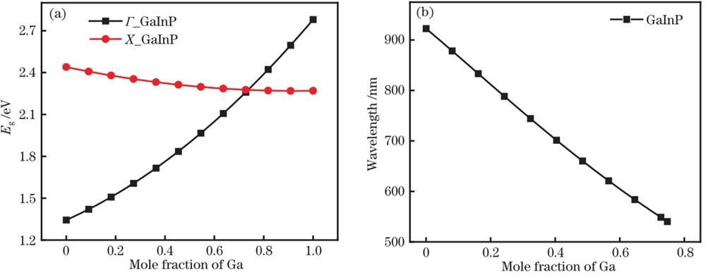
Fig. 1. Band gap energy and laser wavelength of GaInP materials with different Ga mole fractions. (a) Band gap energy; (b) laser wavelength
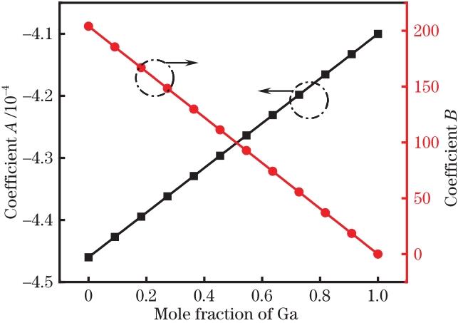
Fig. 2. Coefficients A and B for GaInP materials with different Ga mole fractions
Fig. 3. Lattice constants of different materials. (a) SiGe; (b) GaInP, AlInP; (c) AlGaInP
Fig. 4. Expansion coefficients of SiGe and GaInP materials. (a) SiGe; (b) GaInP
Fig. 5. Variation curve of different lattice constants with temperature
Fig. 6. Optical power and conversion efficiency of 640 nm semiconductor laser
Fig. 7. Output characteristics of 620 nm semiconductor laser on Ge/SixGe1-x substrate
Fig. 8. Variation curve of Ga0.57In0.43P band gap with temperature
Fig. 9. Output characteristics of different quantum well structures
Fig. 10. Peak gain and I-P curve for five structures. (a) Peak gain; (b) I-P curve
|
Table 1. Lattice constants of Si, Ge, GaP, InP and AlP materials
|
Table 2. Expansion coefficients α for Si, Ge, GaP, InP and AlP
|
Table 3. Expansion coefficients of materials
|
Table 4. Parameters and output characteristics of different GaInP quantum wells
|
Table 5. Simulation results for different QW strain structures

Set citation alerts for the article
Please enter your email address
© Copyright 2018-2021 | Chinese Laser Press. All Rights Reserved 沪ICP备15018463号-20