• Opto-Electronic Science
  • Vol. 1, Issue 7, 210011 (2022)
Junyan Chen1、2, Tobias Eul2, Lu Lyu2, Yaolong Li1, Xiaoyong Hu1、4、*, Xingkun Ning3, Shufang Wang3, Martin Aeschlimann2、*, and Qihuang Gong1、4
Author Affiliations
  • 1State Key Laboratory for Mesoscopic Physics & Department of Physics, Collaborative Innovation Center of Quantum Matter & Frontiers Science Center for Nano-optoelectronics, Beijing Academy of Quantum Information Sciences, Peking University, Beijing 100871, China
  • 2Department of Physics and Research Center OPTIMAS, University of Kaiserslautern, Kaiserslautern 67663, Germany
  • 3College of Physics Science & Technology, Hebei University, Baoding 071002, China
  • 4Collaborative Innovation Center of Extreme Optics, Shanxi University, Taiyuan 030006, China
  • show less
    DOI: 10.29026/oes.2022.210011 Cite this Article
    Junyan Chen, Tobias Eul, Lu Lyu, Yaolong Li, Xiaoyong Hu, Xingkun Ning, Shufang Wang, Martin Aeschlimann, Qihuang Gong. Tracing the formation of oxygen vacancies at the conductive LaAlO3/SrTiO3 interface via photoemission[J]. Opto-Electronic Science, 2022, 1(7): 210011 Copy Citation Text show less
    Threshold PEEM imaging of the 2DEG at LaAlO3/SrTiO3 interface. (a) Schematic of the sample structure used in the experiments. (b) The PEEM image of the sample illuminated by the laser beam, which has a wavelength of 210 nm (hν = 5.99 eV). (c) K-space PEEM imaging of the conductive LaAlO3/SrTiO3 interface. The white dash line marks the position of 2DEG states. (d) The photoemission intensity from the polarized regions and the defect-free regions, as marked by the blue and green dashed lines in (b). The insert figure provides a zoom-in view of the photoemission spectrum near the Fermi level.
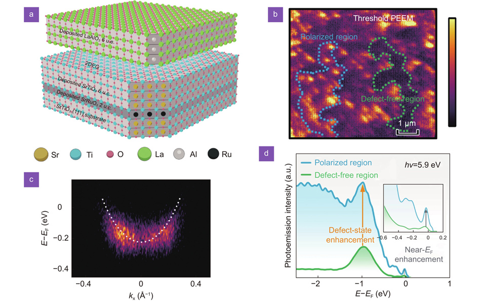
    Fig. 1. Threshold PEEM imaging of the 2DEG at LaAlO3/SrTiO3 interface. (a) Schematic of the sample structure used in the experiments. (b) The PEEM image of the sample illuminated by the laser beam, which has a wavelength of 210 nm ( = 5.99 eV). (c) K-space PEEM imaging of the conductive LaAlO3/SrTiO3 interface. The white dash line marks the position of 2DEG states. (d) The photoemission intensity from the polarized regions and the defect-free regions, as marked by the blue and green dashed lines in (b). The insert figure provides a zoom-in view of the photoemission spectrum near the Fermi level.
    Time-resolved pump–probe measurement of electrons within the two types of interface regions. (a) PEEM image of the sample surface obtained with a 400-nm (hν = 3.1 eV) laser beam. (b) Time-resolved photoemission intensity collected by the lateral regions marked by green and blue dashed lines in (a). Electrons corresponding to initial states 0.4 ± 0.2 eV below EF are extracted and counted. (c) Schematic of the ultrafast electron dynamics within the defect-free interface regions (upper) and the polarized interface regions (bottom). The photoemitted electrons would come from the 2DEG states at the buried interface or the oxygen-related in-gap states at the surface. (d) Layer-resolved density of states obtained by DFT calculations for defect-free interface regions (left column) and the polarized interface regions (right column). The grey dashed square marks the surface states related with the surface oxygen adsorbates.
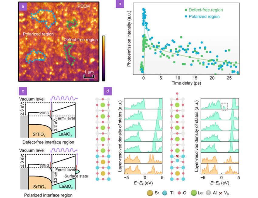
    Fig. 2. Time-resolved pump–probe measurement of electrons within the two types of interface regions. (a) PEEM image of the sample surface obtained with a 400-nm ( = 3.1 eV) laser beam. (b) Time-resolved photoemission intensity collected by the lateral regions marked by green and blue dashed lines in (a). Electrons corresponding to initial states 0.4 ± 0.2 eV below EF are extracted and counted. (c) Schematic of the ultrafast electron dynamics within the defect-free interface regions (upper) and the polarized interface regions (bottom). The photoemitted electrons would come from the 2DEG states at the buried interface or the oxygen-related in-gap states at the surface. (d) Layer-resolved density of states obtained by DFT calculations for defect-free interface regions (left column) and the polarized interface regions (right column). The grey dashed square marks the surface states related with the surface oxygen adsorbates.
    Sequential annealing treatment on the same sample. (a–e) are the PEEM images after each annealing treatment, obtained with a 400-nm (hν = 3.1 eV) laser beam. (f) PEEM image after exposing the sample to oxygen in atmosphere and then annealing at 400 K in UHV. The coverage ratio represents the spatial coverage of the high-photoemission region in the PEEM images.
    Fig. 3. Sequential annealing treatment on the same sample. (a–e) are the PEEM images after each annealing treatment, obtained with a 400-nm ( = 3.1 eV) laser beam. (f) PEEM image after exposing the sample to oxygen in atmosphere and then annealing at 400 K in UHV. The coverage ratio represents the spatial coverage of the high-photoemission region in the PEEM images.
    Time-dependent changes of photoemission intensity within different regions after the illumination of UV light. The two inset schematic figures demonstrate the two influences of UV light on the surface, depleting the surface oxygen adsorbates or the surface lattice oxygen. The former process mainly occurs within the first 20 minutes of UV illumination in the polarized regions, while the latter applies in other cases.
    Fig. 4. Time-dependent changes of photoemission intensity within different regions after the illumination of UV light. The two inset schematic figures demonstrate the two influences of UV light on the surface, depleting the surface oxygen adsorbates or the surface lattice oxygen. The former process mainly occurs within the first 20 minutes of UV illumination in the polarized regions, while the latter applies in other cases.
    Junyan Chen, Tobias Eul, Lu Lyu, Yaolong Li, Xiaoyong Hu, Xingkun Ning, Shufang Wang, Martin Aeschlimann, Qihuang Gong. Tracing the formation of oxygen vacancies at the conductive LaAlO3/SrTiO3 interface via photoemission[J]. Opto-Electronic Science, 2022, 1(7): 210011
    Download Citation