Abstract
![]()
The two-dimensional electron gas (2DEG) generated at the LaAlO3/SrTiO3 interface has been in the focus of oxides research since its first discovery. Although oxygen vacancies play an important role in the generation of the insulator-to-metal transition of the SrTiO3 bare surface, their contribution at the LaAlO3/SrTiO3 interface remains unclear. In this work, we investigated a LaAlO3/SrTiO3 heterostructure with regional distribution of defect-based localized polar sites at the interface. Using static and time-resolved threshold photoemission electron microscopy, we prove that oxygen vacancies are induced near those polar sites, resulting in the increase of carrier density of the 2DEG states. In addition, oxygen-related surface states were uncovered, which we attributed to the release of lattice oxygen during the formation of oxygen vacancies. Such effects are mainly found spatially located around the defect sites at the buried interface, while other regions remain unaffected. Our results confirm that the itinerant electrons induced by oxygen vacancies can coexist with the charge transfer mechanism in the LaAlO3/SrTiO3 heterostructure, together leading to the formation of the metallic interface. These observations provide fundamental insights into the nature of LaAlO3/SrTiO3 interface based 2DEG and unique perspectives for potential applications.
Introduction
Oxide interfaces often exhibit electronic structures quite distinct from bulk properties. In particular, the two-dimensional electron gas (2DEG) found at the interface between the two insulating metal oxides LaAlO3 and SrTiO3 has attracted lots of attention due to its outstanding electronic features including high carrier mobility1, interface magnetism2-5, tunable insulator-to-metal transition6, 7 and two-dimensional superconductivity8, 9. Various theories have been proposed trying to explain the mechanism behind the 2DEG effect. The most famous one is the electron reconstruction raised from the “polar catastrophe” with the polar layer (LaAlO3) over the non-polar material (SrTiO3)10, 11. To compensate such a polar discontinuity, a certain number of charges has to be transferred from the top surface of LaAlO3 to the n-type interface resulting in the formation of a 2DEG around the Fermi energy (EF) and, hence, metallic interface. In addition, oxygen vacancies (VOs) in SrTiO3 are also found to be associated with the confinement of electrons at reduced dimensions. The deletion of lattice oxygen is expected to induced excess electrons, which would fill in the 3D states of neighboring Ti atoms, also contributing to the 2DEG. In particular, VOs succeed in explaining the formation of the 2DEG on the SrTiO3 bare surface12. However, theory calculations suggest that it is energetically unfavorable for VOs to form at the n-type LaAlO3/SrTiO3 interface due to a polar-induced energy barrier13, 14. Therefore, there is still a lack of fundamental understanding about the influence of VOs located at the buried LaAlO3/SrTiO3 interface on the low-dimensional electron confinement.
In this work, localized polar nano-regions (PNRs) are induced at the n-type LaAlO3/SrTiO3 interface by induction of Ti-Sr anti-site defects in the deposited SrTiO3 layer. By using threshold photoemission electron microscopy (PEEM), we are able to selectively focus on the changes of the electrons near the Fermi level at the buried interface. After annealing in an ultra-high vacuum (UHV) environment, we observed the emergence of surface states located within the LaAlO3 band gap, which were resulted from the diffusion of the depleted lattice oxygen during the formation of VOs in the buried SrTiO3 layer. These oxygen-related surface states were spatially overlapped with defect-based PNR sites. Within the regions with VO formation, we also found an increase on the 2DEG density and the local magnetic moments. Our results reveal new fundamental information about the electron confinement in LaAlO3/SrTiO3 interfaces and are of great relevance for the potential applications of 2DEG as they provide new ways to regionally manipulate the electronic properties of 2DEG systems.
Results
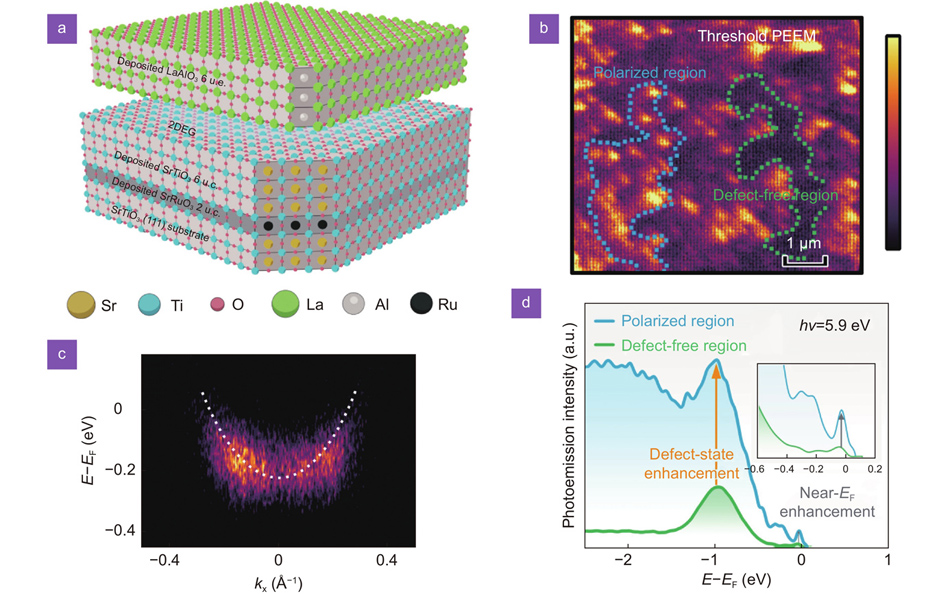
Figure 1(a) shows a sketch of the sample we used in the experiment. Thin SrRuO3 with a thickness corresponding to two unit-cells is first grown by pulsed laser deposition (PLD) on TiO2-terminated (001) SrTiO3 substrates as the bottom electrode. The SrRuO3 electrode is inserted to prevent charging effects during PEEM imaging. Afterwards, we sequentially grow two layers of SrTiO3 and LaAlO3 on the SrRuO3 via the PLD method. Each layer has a thickness of six unit-cells, corresponding to approximately 3 nm, respectively. The thickness of each grown layer is carefully controlled by reflection high-energy electron diffraction (RHEED). The Sr deficiency of the deposited SrTiO3 layer is induced by the strong laser fluence during the growth process, which is reported to lead to the formation of Ti-Sr anti-site defects as well as resulted PNRs with localized ferroelectric polarization15, 16. In our previous study, we have found such defects would lead to localized trapping states and energy-favorable coupling with VOs, while preserving the termination quality of SrTiO317. More details about the sample preparation are described in Section Methods.

Figure 1.Threshold PEEM imaging of the 2DEG at LaAlO3/SrTiO3 interface. (a) Schematic of the sample structure used in the experiments. (b) The PEEM image of the sample illuminated by the laser beam, which has a wavelength of 210 nm (hν = 5.99 eV). (c) K-space PEEM imaging of the conductive LaAlO3/SrTiO3 interface. The white dash line marks the position of 2DEG states. (d) The photoemission intensity from the polarized regions and the defect-free regions, as marked by the blue and green dashed lines in (b). The insert figure provides a zoom-in view of the photoemission spectrum near the Fermi level.
PEEM has been proven to be an ideal tool to study the 2DEG system, with exclusive focus on the confined electrons at reduced dimensions from the insulating bulk materials and the ability for in-situ observation without inducing surface damages12, 18-20. Compared to the tip-based characterization such as atomic force microscopy (AFM), photoemission can directly image the energy distribution of electronic states, which is of great importance in detecting 2DEG. The obtained work function value of our multilayer structure was 2.3 eV, which is consistent with previous reports using a Kelvin probe21. Under the excitation of visible-range laser beam pulse, neither electrons from the SrTiO3 nor from the LaAlO3 valence band can be excited, except for the 2DEG states at the interface. In general, the very low mean free path of the photoelectrons prevents direct access to the electronic properties of buried interfaces. However, we have proven in an earlier work22 that the inelastic mean free path of the photoelectrons at threshold condition can be drastically prolonged in the top dielectric layer. This is caused due to the fact that their excess energy is less than a few electron voltages above the conduction band minimum, which drastically reduces the phase space available for inelastic scattering. Specifically, after photoexcitation of the 2DEG electrons, they will travel through the conducting band of LaAlO3 towards the surface and subsequently couple into the vacuum level.
Figure 1(b) shows an energy-integrated PEEM image after annealing the sample to 900 K in UHV and illuminating it with the normal incident (< 4°) laser beam (hν = 5.9 eV, linear photoemission). We found two types of regions of hundreds of nanometers in size differing in their respective photoemission intensity. Within the bright regions (blue dashed line), the defect-based PNRs at the interface, indicated by the hot spots in the PEEM image, have an influence significant enough to affect the density of states near the Fermi level, while other regions (green dashed line) stay defect-free. In the following text, these two types of regions will be referred to as polarized regions and defect-free regions. Figure 1(c) shows the k-space PEEM imaging of the 2DEG states using the same incident beam, where the focal plane of the photoemitted electrons is imaged instead of the image plane.
In the extracted photoemission spectrum (Fig. 1(d)), we observed a significant increase on the photoemission intensity in the polarized region, which mainly occurs at approximately 0.3 eV and 1.0 eV below the Fermi level. The states at these two binding energies are traditionally attributed to the localized in-gap defect states and quasi-particle 2DEG states12, 23, 24. In the following part, we will demonstrate that these increases on the photoemission intensity in the polarized region are caused by the induction of VOs around the PNR sites located at the interface. Those defect-based PNRs are expected to compensate the polar discontinuity across the buried interface in the neighboring area, lowering the polar-induced energy barrier for the formation of VO. The in-gap defect states were also found in the defect-free regions, which is the result of other intrinsic defects apart from VOs, such as Sr-La anti-site defects at the heterostructure interface. During the high-temperature annealing process, VOs would form around the PNR sites and couple with the Ti-Sr anti-site defects leading to an energetically favorited configuration with a decreased formation energy25, 26. Due to electron correlation, the excess electrons induced by the formation of VOs would not only fill the in-gap defect-based localized states, but also become itinerant and contribute to the 2DEG at the interface27. Moreover, additional structural defects may occur around the PNR sites, since defects tend to form in clusters. With the increase of localized defect density and the decrease of interface homogeneity, the energy barrier for VO formation will be furtherly lifted. The formation of VOs at the buried interface results in additional localized magnetic moments leading to regional enhancement of the 2DEG-based ferromagnetism by increasing the magnetic magnitude. By using the magnetic circular dichroism (MCD) imaging mode of PEEM, we indeed observed an enhancement on the interface ferromagnetic effects within the polarized regions (
Fig. S1) confirming the existence of additional VOs induced around the PNR sites. Further low-enegry electron microscopy measurement suggests the ultra-high flatness of the sample surface, eliminating the possibility of surface inhomogeneity resulting in the two types of regions (
Fig. S8).
To further study the electron dynamics in different interface regions, we performed pump–probe time-resolved PEEM measurements with an 800-nm (hν = 1.55 eV) beam as pump and a 400-nm (hν = 3.1 eV) beam as a probe (see also Section Methods). The pulse length of both beams is approximately 26 fs. During the whole measurement, we did not observe any significant light-induced damages on the sample surface. For reference, a static PEEM image of the same field of view using the 400-nm probe beam only was captured as shown in Fig. 2(a). We extract the photoemission spectrum for electrons from initial states with a binding energy of 0.4 ± 0.2 eV, where the 2DEG states are located. As shown in Fig. 2(b), the difference in ultrafast electron dynamics is striking between the polarized and defect-free regions in the first few ps. Within the whole polarized regions, the decay of the photoemission signal can be divided into two phases, a fast decaying process within the first few ps and a slow decaying process afterwards. Exponential fitting yields a time constant of < 1 ps for the fast process and 15 ps for the slow process. In the defect-free regions, only the slow exponential decay process is observed.
Figure 2.Time-resolved pump–probe measurement of electrons within the two types of interface regions. (a) PEEM image of the sample surface obtained with a 400-nm (hν = 3.1 eV) laser beam. (b) Time-resolved photoemission intensity collected by the lateral regions marked by green and blue dashed lines in (a). Electrons corresponding to initial states 0.4 ± 0.2 eV below EF are extracted and counted. (c) Schematic of the ultrafast electron dynamics within the defect-free interface regions (upper) and the polarized interface regions (bottom). The photoemitted electrons would come from the 2DEG states at the buried interface or the oxygen-related in-gap states at the surface. (d) Layer-resolved density of states obtained by DFT calculations for defect-free interface regions (left column) and the polarized interface regions (right column). The grey dashed square marks the surface states related with the surface oxygen adsorbates.
Although the induction of VOs around the PNR sites and the enhancement effect on 2DEG result in an increase of the density of electron states near Fermi level at the buried interface, this cannot account for the observed fast-decaying peak in the polarized regions. At the buried interface, electrons near the Fermi level would be pumped into the LaAlO3 conducting band under the excitation of the first pump beam, where they gather at the conducting band minimum and slowly decay to a lower energy level due to electron-electron scattering and electron-phonon interactions. With the arrival of the second probe beam, those excited electrons would travel within the conducting band of LaAlO3 to the surface and then be collected by the PEEM system. Such transportation of carriers is based on the diffusion of excited electrons, with a velocity around
, which is calculated by rising edge of the time-resolved PEEM intensity curve. This transport process can explain, where the observed time constant of 15 ps indicates the average lifetime of excited electrons in the conducting band of LaAlO3(Fig. 2(c) top). A reasonable explanation for the observed fast-decaying peak is additional surface states exist on the LaAlO3 top layer around EF in the polarized regions as shown in Fig. 2(c) bottom. These electrons are excited by the pump pulse into a virtual intermediate state in the band gap of LaAlO3 and then photoexcited by the probe pulse. Therefore, the time-resolved photoemission results would be governed by the cross-correlation curve of the pump (800 nm) and probe (400 nm) laser pulse resulting in the fast-decaying peak in Fig. 2(b) (blue dots).
We attribute such surface states in the polarized regions to the diffusion of the depleted lattice oxygen to the LaAlO3 surface. Although the outward diffusion of oxygen ions from SrTiO3 substrate to the upper layer is quite common in SrTiO3-based heterostructures28, 29, it is the first experimental observation of such behavior in conductive LaAlO3/SrTiO3 interface. The existence of oxygen ions on the LaAlO3 surface would compensate the internal electronic field induced by the defect-based excess electrons at the interface, lowering the total energy of the system. In order to support our prediction, we performed density function theory calculations (see Methods). The layer-resolved density of states is shown in Fig. 2(d). Compared to the defect-free LaAlO3/SrTiO3 heterostructure (left column), there are two obvious distinctions caused by the formation of VO around the anti-site defect (right column). There is a negative shift on the electronic states for the SrTiO3 layer near the interface, which results from the energetically favorited coupling between the Ti-Sr anti-site defects and the VOs. More importantly, a peak of oxygen-related surface states raises in the top LaAlO3 layer corresponding to the absorption of oxygen ions on the surface, consisting with our prediction. The calculated value of the band gap is slightly underestimated compared to the experimental results. Since the absorbed oxygen ions come from the depleted lattice oxygen during the formation of VO, such surface states are expected to serve as excellent indicators for VOs located at the buried interface.
In most cases, the depletion process of lattice oxygen is highly dependent on the annealing temperature. To verify such empirical rule, we carry out static PEEM measurement on one sample with successive annealing at different temperatures. Each time the sample is heated to the given temperature in UHV for two minutes and then cooled down back to room temperature. The energy-integrated PEEM images are obtained using 400-nm (hν = 3.1 eV) grazing-incident laser beam, due to better stability of beam path and the convenience of the experiments. As shown in Fig. 3(a), there are only few signs of regional photoemission enhancement in the as-deposited sample. But the coverage of bright regions increases gradually as the annealing temperature increases (Fig. 3(b–e)). Conversely, after exposure to oxygen in atmosphere and then annealing at 400 K in UHV, the sample surface went back to an approximately homogeneous photoemission intensity in the whole field of view (Fig. 3(f)). The appearance of the sample was originally transparent after deposition, then becomes dark after annealing in UHV, and eventually restores the transparency after the exposure to oxygen in atmosphere (
Fig. S2). Such color changes can be attributed to the free carrier absorption of Ti3+ states, which varies on the level of oxidization12.
Figure 3.Sequential annealing treatment on the same sample. (a–e) are the PEEM images after each annealing treatment, obtained with a 400-nm (hν = 3.1 eV) laser beam. (f) PEEM image after exposing the sample to oxygen in atmosphere and then annealing at 400 K in UHV. The coverage ratio represents the spatial coverage of the high-photoemission region in the PEEM images.
As mentioned above, the increased photoemission signal within the affected range of the PNR sites is caused by the increase of the 2DEG as well as the oxygen-related surface states. When exposed to oxygen, the induced VOs may recombine with oxygen in the atmosphere and the oxygen-related surface state are eradicated. Both processes are leading to a suppression of the regional enhancement of photoemission intensity. Therefore, the regional difference in the photoemission signals is eliminated on the sample after exposure to oxygen in atmosphere as shown in Fig. 3(f).
As discussed above, both the 2DEG states at the buried interface as well as the oxygen-related surface states contribute to the photoemission intensity. Further experiments are required to separate these two processes in order to quantify the actual influence of interface VOs on the 2DEG states. Generally, the oxygen-related surface states are more sensitive to external stimulations, compared to the buried interface.
A simple way of surface engineering is exposing the hybrid structure to ultraviolet (UV) light radiation. We applied UV light on the sample surface using a mercury vapor lamp (hν = 4.9 eV). The energy-integrated photoemission intensities obtained using 400-nm (hν = 3.1 eV) are shown in Fig. 4. For the polarized regions, the photoemission intensity decreases notably after the UV illumination within the first 20 minutes. Quite contrary, within the defect-free interface regions, there is a slight increase of the photoemission intensity if the exposure time is less than 15 minutes. For longer exposure time, photoemission intensity in both types of regions continues to decrease with an equal decay rate. In both regions, we observed a slight decrease of the work function after the UV illumination (
Fig. S3).
The different behavior under UV illumination in two separated regions resulte from the different surface conditions. For polarized regions with oxygen-related surface states, the illumination of UV light, which has a photon energy comparable to the bond dissociation energy of oxygen molecules30, removes the additional oxygen ions on the top LaAlO3 surface. This oxygen desorption process leads to a strong reduction of the surface states and, hence, to a reduced photoemission intensity (left inset figure in Fig. 4). This explains the fast drop of the photoemission signal in the polarized regions within the first 25 minutes of UV illumination. Thereafter, most of the additional oxygen ions have been eliminated. For defect-free regions without additional oxygen ions on the top LaAlO3 surface, UV light depletes lattice oxygen within the first few layers of LaAlO3 and induces VOs on the top LaAlO3 surface (right inset figure in Fig. 4). Considering the p-type nature of this UV light modified top LaAlO3 surface, a small amount of surface defects slightly increases the photoemission intensity via an enhanced charge transfer process to the interface. After 20 minutes of UV illumination, the increasing density of defects starts to destroy the crystal structure in both regions. Such an irreversible damage caused by strong UV light illumination has also been reported in other 2DEG systems31, 32. This continuous accumulation of surface defects can explain the following slow decrease of photoemission intensity in both regions.
Figure 4.Time-dependent changes of photoemission intensity within different regions after the illumination of UV light. The two inset schematic figures demonstrate the two influences of UV light on the surface, depleting the surface oxygen adsorbates or the surface lattice oxygen. The former process mainly occurs within the first 20 minutes of UV illumination in the polarized regions, while the latter applies in other cases.
Conclusions
Our results indicate that within the polarized regions affected by PNRs, the formation of VO at the buried interface influences the electronic band structure at two different regions: In the interface region an enhancement of 2DEG has been observed and on the top LaAlO3 surface oxygen-related surface states due to the release of lattice oxygen. In general, the formation of VOs at the n-type LaAlO3/SrTiO3 interface is prohibited due to the polar-induced energy barrier13, 33, 34. However, this limitation is expelled around the defect-based PNRs in the SrTiO3, where the localized ferroelectric polarization compensates the intern electronic field in the LaAlO3 layer15, 25, 26, 35. Around the PNR sites, carriers of the 2DEG states are provided by the excess electrons induced by the formation of VOs. Quite contrary, within the defect-free regions, beyond the affected range of the PNRs, the formation of the metallic interface is attributed to the well-known charge transfer from the LaAlO3 top surface to the buried interface. Whether the two origins for the 2DEG coexist in the same or different nano-domains during the formation of the 2DEG cannot be deduced from our data due to the limitation of the spatial resolution of our PEEM system (<30 nm).
Our observed oxygen-related surface states are supported by a distinctive fast-decay component in ultrafast pump–probe PEEM investigations. By inducing UV illumination, we managed to separate the contribution of 2DEG states at the buried interface from the oxygen-related surface states to the photoemission signal. Our results reveal the importance of VOs in the insulator-to-metal transition of the LaAlO3/SrTiO3 interface in addition to the polar-induced charge transferring mechanism. Such a scenario may also apply to other systems with low-dimensional electron confinement.
Since 2DEG located at the buried interface is traditionally beyond the detective range of a point-by-point characterization method such as AFM, our finding provides us with a new way to investigate the 2DEG evolution deep from the surface by studying the changes of surface states. Nevertheless, the dynamics of defects, as well as defect-based electronic states, are of great importance in the formation of low-dimensional electron confinement, which should be taken into consideration in future studies of SrTiO3-based 2DEG systems.
Methods
Sample preparation. The SrTiO3 (001) substrate is first treated with a buffered hydrofluoric acid etch and then annealed in oxygen at 1050 °C to create an atomically smooth surface with TiO2 termination. SrRuO3 with 2-unit-cell thickness, SrTiO3 with 6-unit-cell thickness and LaAlO3 with 6-unit-cell thickness were sequentially grown on the substrate via PLD growth. All the growth processes were performed at a temperature of 750 °C and an oxygen pressure of 10−6 mbar. The KrF excimer laser beam used for the SrTiO3 growth has a wavelength of 248 nm and an energy density of ~2 J/cm2. Such a high laser fluence during PLD growth is reported to result in the Sr deficiency and the induction of Ti-Sr anti-site defects in the deposited SrTiO3 layer15, 16, 36. The in-situ RHEED measurement assures the n-type interface in the grown LaAlO3/SrTiO3 heterostructure with Ti-O and La-O termination across the interface.
PEEM measurement. Our experimental setup consists of a photoemission electron microscope (NI-IS-PEEM, Focus GmbH) in combination with a time-of-flight (ToF) electron energy analyzer. The sample is illuminated under near normal incidence (4°) or grazing incidence (65°). As a light source, we use the first (840 nm), second (SHG, 420 nm) or fourth (FHG, 210 nm) harmonics of a commercial mode locked Ti:Sa oscillator (MaiTai, Spectra Physics) with a repetition rate of 80 MHz. During the measurement, the samples were placed in an UHV environment with pressure below 10–10 mbar. When performing the annealing process, the sample has been heated by a filament installed in a manipulator inside the UHV system. The overall energy resolution of the PEEM was about 75 meV.
Density functional theory calculation. The calculations were carried out based on the local-density approximation (LDA) as implemented in the ABINIT code37, 38. A 6 × 6 × 6 Monkhorst–Pack k-point mesh was used in the calculation. Such approach has been successfully used to demonstrate the electronic and structural properties of perovskite heterostructures39, 40. The 5-unit-cell LaAlO3 layer was placed over 5-unit-cell SrTiO3 to simulate the sample structure, and a vacuum layer with a thickness corresponding to 20 unit-cells was induced on the top surface to separate the supercell from the periodicity in the vertical direction. We allowed full atomic relaxations except for the first SrTiO3 layer. The systematic underestimation of the band gap was resulted from the assumption of LDA. The layer-resolved density of states was obtained by summing the local density of states of the atoms located in each lattice layer.
This work was supported by the National Key Research and Development Program of China under Grant Nos. 2018YFB2200403 and 2018YFA0704404, and the National Natural Science Foundation of China under Grant Nos. 61775003, 11734001, 91950204, 11527901, and Beijing Municipal Science & Technology Commission No. Z191100007219001. In addition, T.E and M.A acknowledge financial support by the Deutsche Forschungsgemeinschaft (DFG, German Research Foundation) – TRR 173 – 268565370 (projects A02).
Supplementary information for this paper is available at https://doi.org/10.29026/oes.2022.210011
The authors declare no competing financial interests.