• Photonics Research
  • Vol. 5, Issue 2, A23 (2017)
Christopher A. Bower1、*, Matthew A. Meitl1, Brook Raymond1, Erich Radauscher1, Ronald Cok1, Salvatore Bonafede1, David Gomez1, Tanya Moore1, Carl Prevatte1, Brent Fisher1, Robert Rotzoll1, George A. Melnik1, Alin Fecioru2, and António José Trindade2
Author Affiliations
  • 1X-Celeprint Inc., Research Triangle Park, North Carolina 27709, USA
  • 2X-Celeprint Ltd., Cork, Ireland
  • show less
    DOI: 10.1364/PRJ.5.000A23 Cite this Article Set citation alerts
    Christopher A. Bower, Matthew A. Meitl, Brook Raymond, Erich Radauscher, Ronald Cok, Salvatore Bonafede, David Gomez, Tanya Moore, Carl Prevatte, Brent Fisher, Robert Rotzoll, George A. Melnik, Alin Fecioru, António José Trindade. Emissive displays with transfer-printed assemblies of 8  μm × 15  μm inorganic light-emitting diodes[J]. Photonics Research, 2017, 5(2): A23 Copy Citation Text show less
    Illustration of a conceptual μILED display.
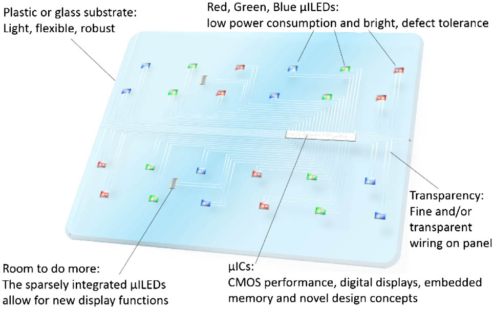
    Fig. 1. Illustration of a conceptual μILED display.
    (a) Transfer stamp retrieves an array of micro-devices from a native wafer with densely packed micro-devices and (b) transfers the dispersed micro-devices onto the receiving substrate. (c) A transfer stamp is illustrated in cross section and (d) in a photograph of a transfer stamp with a 100 mm×50 mm active area. The inset shows an electron micrograph of the surface relief on the elastomer stamp.
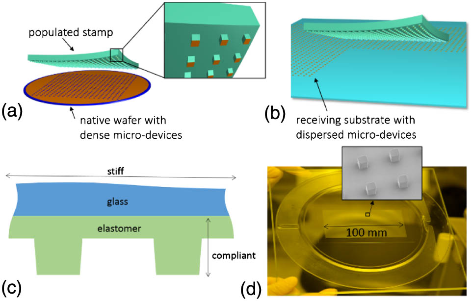
    Fig. 2. (a) Transfer stamp retrieves an array of micro-devices from a native wafer with densely packed micro-devices and (b) transfers the dispersed micro-devices onto the receiving substrate. (c) A transfer stamp is illustrated in cross section and (d) in a photograph of a transfer stamp with a 100  mm×50  mm active area. The inset shows an electron micrograph of the surface relief on the elastomer stamp.
    (a) Illustration of the process steps for making printable μILEDs. (b) Optical micrograph of a μILED wafer, and (c) electron micrograph of a released, ready-to-retrieve, μILED.
    Fig. 3. (a) Illustration of the process steps for making printable μILEDs. (b) Optical micrograph of a μILED wafer, and (c) electron micrograph of a released, ready-to-retrieve, μILED.
    (a) Illustration of passive-matrix μILED display fabrication. (b) Optical micrograph taken after printing and via formation, and (c) optical micrograph of the completed passive-matrix display.
    Fig. 4. (a) Illustration of passive-matrix μILED display fabrication. (b) Optical micrograph taken after printing and via formation, and (c) optical micrograph of the completed passive-matrix display.
    (a) Photograph of a blue 10 mm×10 mm, 254 PPI, passive-matrix display, and (b) higher magnification image showing the pixels during operation. (c) Photograph of a full-color 20 mm×20 mm, 127 PPI, passive-matrix display, and (d) close-up image of the pixels during operation.
    Fig. 5. (a) Photograph of a blue 10  mm×10  mm, 254 PPI, passive-matrix display, and (b) higher magnification image showing the pixels during operation. (c) Photograph of a full-color 20  mm×20  mm, 127 PPI, passive-matrix display, and (d) close-up image of the pixels during operation.
    (a) Luminance of a 254 PPI passive-matrix display as a function of the duty cycle, or number of active rows. (b) Luminance measured versus viewing angle. (c) Photograph of a 127 PPI μILED with a 9 V battery in the background illustrating the transparency of the display. (d) Measured optical transmission versus wavelength for the 127 PPI display. (e),(f) Photographs of the plastic, flexible, passive-matrix μILED display.
    Fig. 6. (a) Luminance of a 254 PPI passive-matrix display as a function of the duty cycle, or number of active rows. (b) Luminance measured versus viewing angle. (c) Photograph of a 127 PPI μILED with a 9 V battery in the background illustrating the transparency of the display. (d) Measured optical transmission versus wavelength for the 127 PPI display. (e),(f) Photographs of the plastic, flexible, passive-matrix μILED display.
    (a) Photograph of the 254 PPI full-color display that was used for the subpixel yield measurement, and (b)–(d) individual photographs with the respective subpixels (red, green, and blue) turned on separately.
    Fig. 7. (a) Photograph of the 254 PPI full-color display that was used for the subpixel yield measurement, and (b)–(d) individual photographs with the respective subpixels (red, green, and blue) turned on separately.
    (a) Process sequence for making the active-matrix μILED display. (b) Optical micrograph of a single pixel after printing the μILEDs and μICs. (c) Electron micrograph of a fully processed active-matrix display. (d) Circuit diagram illustrating the display control architecture. (e) Photograph of the 127 PPI active-matrix display in operation. (f) Color gamut of the display.
    Fig. 8. (a) Process sequence for making the active-matrix μILED display. (b) Optical micrograph of a single pixel after printing the μILEDs and μICs. (c) Electron micrograph of a fully processed active-matrix display. (d) Circuit diagram illustrating the display control architecture. (e) Photograph of the 127 PPI active-matrix display in operation. (f) Color gamut of the display.
    Christopher A. Bower, Matthew A. Meitl, Brook Raymond, Erich Radauscher, Ronald Cok, Salvatore Bonafede, David Gomez, Tanya Moore, Carl Prevatte, Brent Fisher, Robert Rotzoll, George A. Melnik, Alin Fecioru, António José Trindade. Emissive displays with transfer-printed assemblies of 8  μm × 15  μm inorganic light-emitting diodes[J]. Photonics Research, 2017, 5(2): A23
    Download Citation