Christopher A. Bower1、*, Matthew A. Meitl1, Brook Raymond1, Erich Radauscher1, Ronald Cok1, Salvatore Bonafede1, David Gomez1, Tanya Moore1, Carl Prevatte1, Brent Fisher1, Robert Rotzoll1, George A. Melnik1, Alin Fecioru2, and António José Trindade2
Abstract
Displays using direct light emission from microscale inorganic light-emitting diodes (μILEDs) have the potential to be very bright and also very power efficient. High-throughput technologies that accurately and cost-effectively assemble microscale devices on display substrates with high yield are key enablers for μILED displays. Elastomer stamp transfer printing is such a candidate assembly technology. A variety of μILED displays have been designed and fabricated by transfer printing, including passive-matrix and active-matrix displays on glass and plastic substrates.1. INTRODUCTION
Precise and rapid assembly of miniature wafer-fabricated components onto panel substrates enables a hybrid manufacturing approach for high-performance, multi-functional displays. Control circuits, light emitters, sensors, and other micro-components formed at high densities on crystalline wafer substrates employ a variety of processes and materials that are incompatible with glass and plastic panel substrates. Displays assembled from those micro-components can therefore have performance attributes that are difficult to achieve with panel processes alone. Figure 1 illustrates a portion of a conceptual display with assemblies of high-performance micro-devices. The illustration shows a cluster of four pixels driven by a single microscale integrated circuit (μIC), where each pixel contains six microscale inorganic light-emitting diodes (μILEDs). In this illustration, the μIC also controls two micro-sensors demonstrating how sparsely integrated μILEDs enable new functions in the panel system. The realization of such displays requires a mass transfer technology that can rapidly and precisely assemble large numbers of micro-components onto the display substrate.
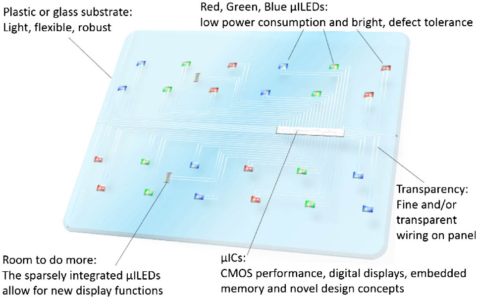
Figure 1.Illustration of a conceptual μILED display.
Light-emitting diodes (LEDs) made from inorganic crystalline semiconductors are the brightest, longest-lived, and most efficient light emitters available for displays. Inorganic LEDs are used as backlights for liquid crystal displays (LCDs) and front-lights for reflective displays. Surface-mountable packaged LEDs are the compact pixels within large public video displays. There is growing interest in micrometer-scale LED chips as direct light emitters within the pixels of everyday displays, such as TVs and smartphones. Here we present a variety of displays made using assemblies of transfer-printed μILEDs and μICs.
Transfer printing with elastomer stamps is a broadly applicable and practical mass transfer technique that was originally developed in Professor John Roger’s Laboratory at the University of Illinois, Urbana–Champaign [1,2]. Over the last decade, the technology has been continuously advanced by commercial groups and those looking to demonstrate new classes of devices that leverage micro-assembly. Transfer-print technology has also been applied in photovoltaics [3], general lighting [4], magnetic storage [5], optical communications [6], bio-integrated optoelectronics [7], and displays [8–10]. In 2009, Rogers and his colleagues demonstrated deformable and semitransparent prototype displays using transfer-printed μILEDs [8].
Sign up for Photonics Research TOC. Get the latest issue of Photonics Research delivered right to you!Sign up now
In transfer printing, a stamp made of glass and the viscoelastic elastomer, polydimethylsiloxane (PDMS), serves as a carrier to transfer arrays of devices from their native substrate onto non-native destination substrates. The process exploits rate-dependent, switchable adhesion between the device and elastomer to pick up and print arrays of micrometer-scale devices [2,11,12]. As illustrated in Figs. 2(a) and 2(b), relief structure on the stamp surface enables the deterministic dispersion of devices from dense arrays on a native substrate to sparse arrays on non-native destination substrates. The transfer process works at room temperature and uses no solvents or vacuum. It is applicable to almost any destination substrate with a receiving surface, e.g., glass, ceramics, plastics, and other semiconductors.

Figure 2.(a) Transfer stamp retrieves an array of micro-devices from a native wafer with densely packed micro-devices and (b) transfers the dispersed micro-devices onto the receiving substrate. (c) A transfer stamp is illustrated in cross section and (d) in a photograph of a transfer stamp with a active area. The inset shows an electron micrograph of the surface relief on the elastomer stamp.
Some key attributes of transfer-print technology arise from the nature of the transfer element. The transfer stamp, illustrated in Fig. 2(c), is made from glass and elastomer using a simple inexpensive injection-molding technique [13]. The compliant elastomer surface allows the stamp to physically contact surfaces that are not perfectly flat. It is naturally soft, facilitating damage-free transfer of fragile, thin, micrometer-scale devices. The stamp is engineered to be stiff in lateral directions, enabling high placement accuracy. Earlier work demonstrated that arrays of 46,080 μICs could be printed with alignment distributions of [14]. Recent studies demonstrate that stamps can be robust and maintain their process yield and placement performance over tens of thousands of print cycles [13]. Moreover, the stamp is naturally transparent, allowing machine optics to look through the stamp to facilitate accurate alignment of the micro-devices to the receiving substrate. The stamp is also scalable to large sizes, with 150 mm scale stamps already demonstrated [13]. Figure 2(d) is a photograph of a stamp with a active surface. The stamp integrates into simple, highly scalable motion-plus-optics automated machinery.
2. PRINTABLE μILEDS
Transfer-print-compatible devices have specialized designs that allow them to be retrieved from their native substrate using elastomer stamps. These design and process strategies have been demonstrated for a wide variety of optoelectronic devices, including μILEDs, and are reviewed elsewhere [15]. The first printable μILEDs were red-light emitting, used (Al)InGaP quantum wells, and were grown on GaAs substrates [8]. The total thickness of the active layers was . The active layers were grown on top of a 1.5 μm thick layer of , which served as a sacrificial release layer. In that work, the μILEDs were lateral devices and ranged in size from to . Polymer photoresist structures were defined to anchor the μILEDs to the GaAs substrate, so that the μILEDs remained undisturbed when the sacrificial layer was removed. These polymer features, used to tether the μILED to the substrate, break during the μILED retrieval process. Conceptually similar strategies have been employed for vertical red μILEDs [16] and for μILEDs based on InGaN grown on silicon (1 1 1) [4] and sapphire [17]. On sapphire, multi-phase layers formed on the top of the μILEDs serve as release layers after bonding and laser lift-off to remove the sapphire substrate. Chemical etching selectively removes one or more phases from the release layer, leaving the remaining phases as anchors to keep the released device in its original placement prior to retrieval by stamp [17]. In the GaN-on-silicon system, anisotropic etching of the substrate in hot aqueous base undercuts the LEDs but leaves anchoring structures bounded by slow-etching planes attached to the substrate [4]. In that work, narrow GaN tethers that attach the μILEDs to the anchors break during the retrieval process. The devices used lateral contacting schemes and ranged in size from to .
To achieve full-color μILED displays, we have extended these concepts to smaller, red, green, and blue, lateral μILEDs with sizes ranging from [10] to . The process steps for fabricating the μILEDs are illustrated in Fig. 3(a). The red μILED epitaxial growth takes place on a GaAs substrate and includes an AlInP sacrificial layer, a transparent current spreading layer, and (Al)InGaP quantum wells. The green and blue μILED growth takes place on a Si (1 1 1) wafer and also includes transparent current spreading layers underneath the quantum wells. The Si (1 1 1) serves as the sacrificial material for the printable green and blue μILEDs. The mesas are formed using photoresist etch masks and reactive ion etching. The active area of the μILED is defined by the mesa through the junction and is approximately for these devices. The ohmic contacts are formed using lift-off patterning, evaporation, and annealing. For all colors, deposited and patterned inorganic dielectric layers are used to anchor and tether the μILEDs during and after removal of the underlying sacrificial materials. An additional metallization step allows the formation of larger and thicker contact pads, and can also serve as a light reflector. Figure 3(b) is an optical micrograph of red μILEDs that are ready for etching the underlying sacrificial layer. Figure 3(c) is a top-down electron micrograph of a fully fabricated and undercut (ready to retrieve) μILED.
Figure 3.(a) Illustration of the process steps for making printable μILEDs. (b) Optical micrograph of a μILED wafer, and (c) electron micrograph of a released, ready-to-retrieve, μILED.
3. PASSIVE-MATRIX μILED DISPLAYS
In a passive-matrix display, each row (common electrode) is activated sequentially, while the other rows are held in a reverse-bias/non-select off state. The information display data is delivered to the individual subpixels through the column wires. When the rows are scanned at a high enough frequency, the viewer experiences a flicker-free image. The brightness of a passive-matrix display is dictated by the burst of light that each row can produce during its “on/select” time. For a display with 100 rows, the maximum brightness seen by a viewer will be 1% of the brightness capability of each row of pixels. To achieve a 500 nit 100-row passive-matrix display, each row must be capable of emitting 50,000 nits. The ability to achieve such high luminance with robustness and long lifetime make μILEDs perfectly suited for passive-matrix display applications.
Transfer-printed assemblies of μILEDs can be formed into emissive passive-matrix displays. These simple displays consist of only the μILEDs, thin-film metal wires, and a transparent glass or plastic substrate. Figure 4(a) illustrates the display fabrication process. An elastomer stamp transfers arrays of μILEDs from their native source wafer onto a non-native display substrate that has previously patterned display column wires covered by a dielectric film and a thin polymer resin on top of the dielectric film to aid the transfer process. After transfer printing, standard photolithography and reactive ion etching opens vias through the dielectric layers, and another metal layer is applied and patterned to form the common/row electrode. Figure 4(b) is an optical micrograph of the display following printing and via formation. The second thin-film metal layer, which contacts the μILED cathodes, also makes interconnections between the μILED anodes and the display column wires, as shown in Fig. 4(c). In these displays, the μILEDs are designed to emit light through the transparent display substrate. These displays use a commercially available passive-matrix organic LED (OLED) driver chip from Solomon Systech (SSD 1351). The driver chip and the flex cable are attached to the glass display panel using thermal compression bonding with an anisotropic conductive film (ACF).
Figure 4.(a) Illustration of passive-matrix μILED display fabrication. (b) Optical micrograph taken after printing and via formation, and (c) optical micrograph of the completed passive-matrix display.
Figure 5(a) is a photograph of a 254 PPI, display where blue μILEDs were printed in each subpixel. In this case, the entire display area is populated in a single print step per color/subpixel; thus, 10,000 μILEDs are transferred during each print sequence. Figure 5(b) is a higher magnification view showing the individual pixels during display operation. Figure 5(c) is a photograph of a larger, full-color 127 PPI, display. In this case, each is populated in a single print step per color, meaning that the display is completed in 12 print steps. Figure 5(d) is a higher magnification image showing the pixels during display operation.
Figure 5.(a) Photograph of a blue , 254 PPI, passive-matrix display, and (b) higher magnification image showing the pixels during operation. (c) Photograph of a full-color , 127 PPI, passive-matrix display, and (d) close-up image of the pixels during operation.
The display brightness was evaluated using a luminance meter (Konica Minolta LS-110). The brightness of a passive-matrix display is related to the duty cycle, or the number of active rows. Figure 6(a) shows the measured luminance versus duty cycle for the full white image of a full-color 254 PPI display. One anticipated benefit of μILED displays is a very wide viewing angle. Figure 6(b) shows the measured luminance versus viewing angle (both polar and azimuth) for the same passive-matrix μILED display with a full white image. Figure 6(c) is a photograph of the blue 127 PPI display, with a 9 V battery in the background. These displays are very transparent. The major sources of obscuration are reflections and absorption from the metal row and column wires, and the reflections at display/air interfaces. Figure 6(d) shows a measurement of the optical transmission through the display versus wavelength. The dashed line of Fig. 6(d) plots the ratio of the display transmittance to the transmittance of a bare glass substrate. At these resolutions, it is practical to consider display designs with an optical transmission exceeding 90% using antireflection coatings at the air interfaces and narrower traces or more transparent wiring materials.
Figure 6.(a) Luminance of a 254 PPI passive-matrix display as a function of the duty cycle, or number of active rows. (b) Luminance measured versus viewing angle. (c) Photograph of a 127 PPI μILED with a 9 V battery in the background illustrating the transparency of the display. (d) Measured optical transmission versus wavelength for the 127 PPI display. (e),(f) Photographs of the plastic, flexible, passive-matrix μILED display.
Transfer-printed μILEDs are well-suited for plastic displays. Unlike OLED materials, μILEDs are not sensitive to air or water vapor, and they do not require the complex barrier systems designed to protect OLEDs from the environment. Simple plastic displays were made by essentially following the same display fabrication routine as used on glass. To prepare the display substrate, a 125 μm thick sheet of thermally stabilized plastic (Dupont Teijin PEN) was attached to a glass carrier using thermal release tape (Revalpha). Once attached to the glass carrier, the same display fabrication sequence was followed. The transfer-print process occurs at room temperature, and the maximum temperature required in the display fabrication process is 150°C, for curing the polymer resin. At the conclusion of the display fabrication, the display was released from the glass carrier wafer by heating it on a hot plate to a temperature above the tape release temperature (). Figures 6(e) and 6(f) are photographs of a plastic μILED display (, 254 PPI). The total thickness of the display is .
The fabrication of the devices presented here occurred in a research laboratory and development environment not optimized for high-yield processing. Nevertheless, the transfer-print yields of these μILEDs commonly exceed 99.9% and often approach 99.99%. The functional subpixel yields for the display shown in Fig. 7(a) were measured by analyzing digital photographs of the respective red, green, and blue flat fields. These photographs are shown in Figs. 7(b)–7(d).
Figure 7.(a) Photograph of the 254 PPI full-color display that was used for the subpixel yield measurement, and (b)–(d) individual photographs with the respective subpixels (red, green, and blue) turned on separately.
In this example, the measured subpixel yields were 99.7% for red, 99.5% for green, and 99.7% for blue. The μILED fabrication processes are primary root-cause contributors to yield loss. Improved manufacturing controls and environment are expected to significantly improve functional yield.
The bright, air-stable emitters of μILED displays enable unique strategies for defect tolerance and repair. Importantly, air-stability allows physical corrective action to defective pixels prescribed by display-level tests from fully operational panels. Testing in this manner can use very high-throughput screening by optical feedback from every pixel and provides an end-of-line quality check for all intra-panel processes, including emitter fabrication, transfer, and interconnection. The high luminance levels of μILEDs allow them to supply sufficient light for the display while occupying only a small fraction (e.g., 1% or lower) of the pixel area, leaving much of the pixel’s area open to support the physical structures associated with repair actions. Earlier work [10] demonstrated how defective μILEDs can be simply removed from fully operational displays mechanically. This same work illustrated how redundant μILEDs might be selected electronically and used for perceptual masking of defects in μILED displays. Furthermore, the small fill factor and ability to optically mask defects using nearby light emitters opens pathways for additive repair by physical insertion of replacement emitters inside non-operational pixels. Recently, micro-components with sharp, metallic, pressure concentrators have been interconnected with metallized substrates during elastomer transfer printing [18].
4. μILED DISPLAYS WITH μICS
Active-matrix displays with an associated electronic drive circuit for each subpixel can be larger, brighter, and more efficient than passive-matrix displays [19]. Today, the pixel control circuits are fabricated using thin-film transistor (TFT) technology [20]. In TFT technology, amorphous silicon or other non-crystalline semiconductors are deposited as thin-films onto large-format panel substrates, and are then converted into transistors using panel-level lithography and metallization processes. TFT technology provides the necessary performance for driving non-emissive LCDs, where the pixel circuit is a simple voltage switch. Emissive displays, such as OLED and μILED, are more challenging because each pixel circuit must supply an accurate and uniform electrical drive current to all of the LEDs. After decades of investment and development, active-matrix OLED displays using low-temperature poly-silicon (LTPS) TFT technology have recently been commercialized by a few companies [21]. The pixel circuits using LTPS TFT technology are designed to compensate for materials’ non-uniformity and instability, and typically contain five to seven transistors and usually require charge storage on a capacitor for a full frame period. The capacitor becomes a large portion of the pixel area resulting in yield-limiting process defects and limited data transfer rates.
In sharp contrast to TFT technology, modern integrated circuits are formed in crystalline silicon at wafer level and do not suffer from materials-related instabilities or non-uniformities, and achieve massive cost-reduction through miniaturization. Here we demonstrate a prototype active-matrix μILED display enabled by transfer-printed μICs.
A full-color, 127 PPI, active-matrix display was produced by transfer printing both μICs and μILEDs. The process sequence is illustrated in Fig. 8(a). Similar to the passive-matrix display, the fabrication starts by deposition and patterning of a first thin-film metal level on a transparent substrate followed by deposition of an insulating dielectric layer and polymer resin. Next, an elastomer stamp with a relief pattern accurately transfers the μILEDs and μICs onto the display. This display uses the same lateral μILEDs that were used in the passive-matrix displays. The μICs were fabricated using a commercially available 180 nm SOI-CMOS process [22] and are made print-ready by anisotropic etching of the handle silicon underneath the buried oxide layer of the μIC. Like the μILEDs, the μICs remain anchored to regions of the source wafer that are not undercut, and breakable tethers are formed by inorganic dielectric structures. The μICs have lateral dimensions of and are 6 μm thick. The display is completed by forming a second metal level that connects to the surface electrodes (IOs) on the micro-components and to the first metal through a via in the dielectric. The second metal level is fabricated using a semi-additive electroplated copper thin-film [23] to accommodate the topography of the μICs. A custom flex cable is ACF-bonded to the display, and a Xilinx FPGA development kit along with a custom daughter-board is used to control the display. There are no data/select multiplexing row or column circuits in this prototype display.
Figure 8.(a) Process sequence for making the active-matrix μILED display. (b) Optical micrograph of a single pixel after printing the μILEDs and μICs. (c) Electron micrograph of a fully processed active-matrix display. (d) Circuit diagram illustrating the display control architecture. (e) Photograph of the 127 PPI active-matrix display in operation. (f) Color gamut of the display.
An optical micrograph of a single pixel is shown in Fig. 8(b). This image is taken after transfer-printing of the μILEDs and μICs onto the display. The pixel was designed to showcase the potential for redundancy in μILED displays. In this case, each pixel contains two red, two green, and two blue μILEDs, and each pixel contains two pixel μICs. In this design, each μIC controls a single red, green, and blue μILED. Figure 8(c) is an electron micrograph of the completed display.
μICs provide the display designer with a myriad of control architecture possibilities. The architecture employed here is illustrated in Fig. 8(d). In this display, digital data is transmitted to the μICs and stored in a three-stage shift register. The μICs have circuits designed to locally generate the drive current for the μILEDs. In this display, the μILEDs always experience a constant drive current, and the intensity is controlled using pulse width modulation (PWM). In this case, PWM pulses are applied to the across the entire display.
A photograph of an active-matrix μILED display in operation is shown in Fig. 8(e). A benefit of PWM is that the μILEDs always experience the same drive conditions, which means that it should be possible to design displays where the μILEDs operate near optimal power conversion efficiencies, and the potential for color shift attributed to analog current drive schemes is eliminated. The color performance of the active-matrix μILED display was measured in an integrating sphere (Labsphere). Figure 8(f) illustrates the measured display color coordinates along with the Rec. 2020 gamut in the (, ) representation. The color gamut of the μILED display has a 93.3% overlap with the Rec. 2020 gamut, and has 107.1% of the Rec. 2020 area.
The display design is the first known use of a local current generator within each pixel. The display operates with row clock rates in excess of 20 MHz and with frame rates up to 180 Hz. The μIC is the smallest known mixed-signal CMOS integrated circuit to be manufactured and interconnected to date.
5. CONCLUSIONS
Displays based on assemblies of microscale, wafer-fabricated components, such as μILEDs and μICs, can have levels of power efficiency, brightness, and lifetime that are inaccessible to conventional flat-panel display technologies. The required assembly technology must be high-yield, cost-effective, and well-suited for handling micrometer-scale devices. Elastomer stamp transfer printing is an assembly technology with the potential to meet these demands. Here, μILEDs transfer printed to glass and plastic substrates in a research laboratory setting formed the basis of small passive-matrix and active-matrix displays.
References
[1] E. Menard, K. J. Lee, D.-Y. Khang, R. G. Nuzzo, J. A. Rogers. A printable form of silicon for high performance thin film transistors on plastic substrates. Appl. Phys. Lett., 84, 5398-5400(2004).
[2] M. A. Meitl, Z.-T. Zhu, V. Kumar, K. J. Lee, X. Feng, Y. Y. Huang, I. Adesida, R. G. Nuzzo, J. A. Rogers. Transfer printing by kinetic control of adhesion to an elastomeric stamp. Nat. Mater., 5, 33-38(2006).
[3] X. Sheng, C. A. Bower, S. Bonafede, J. Wilson, B. Fisher, M. Meitl, H. Yuen, S. Wang, L. Shen, A. R. Banks, C. J. Corcoran, R. G. Nuzzo, S. Burroughs, J. A. Rogers. Printing-based assembly of quadruple-junction four-terminal microscale solar cells and their use in high-efficiency modules. Nat. Mater., 13, 593-598(2014).
[4] H. Kim, E. Brueckner, J. Song, Y. Li, S. Kim, C. Lu, J. Sulking, K. Choquette, Y. Huang, R. G. Nuzzo, J. A. Rogers. Unusual strategies for using indium gallium nitride grown on silicon (111) for solid-state lighting. Proc. Natl. Acad. Sci. USA, 108, 10072-10077(2011).
[5] J. Justice, C. A. Bower, M. Meitl, M. B. Mooney, M. A. Gubbins, B. Corbett. Wafer scale integration of III V lasers on silicon using transfer printing of epitaxial layers. Nat. Photonics, 6, 612-616(2012).
[6] R. Loi, J. O’Callaghan, B. Roycroft, C. Robert, A. Fecioru, A. J. Trindade, A. Gocalinska, E. Pelucchi, C. A. Bower, B. Corbett. Transfer printing of AlGaInAs/InP etched facet lasers to Si substrates. IEEE Photon. J., 8, 1-10(2016).
[7] D. H. Kim, N. Lu, R. Ghaffari, J. A. Rogers. Inorganic semiconductor nanomaterials for flexible and stretchable bio-integrated electronics. NPG Asia Mater., 4, e15(2012).
[8] S.-I. Park, Y. Xiong, R.-H. Kim, P. Elvikis, M. Meitl, D.-H. Kim, J. Wu, J. Yoon, C.-J. Yu, Z. Liu, Y. Huang, K.-C. Hwang, P. Ferreira, X. Li, K. Choquette, J. A. Rogers. Printed assemblies of inorganic light-emitting diodes for deformable and semitransparent displays. Science, 325, 977-981(2009).
[9] C. A. Bower, E. Menard, S. Bonafede, J. W. Hamer, R. S. Cok. Transfer-printed microscale integrated circuits for high performance display backplanes. IEEE Trans. Compon. Packag. Manuf., 1, 1916-1922(2011).
[10] M. Meitl, E. Radauscher, S. Bonafede, D. Gomez, T. Moore, C. Prevatte, B. Raymond, B. Fisher, K. Ghosal, A. Fecioru, A. J. Trindade, D. Kneeburg, C. A. Bower. 55‐1: Invited paper: passive matrix displays with transfer‐printed microscale inorganic LEDs. SID Symp. Dig. Tech. Pap., 47, 743-746(2016).
[11] A. Carlson, H.-J. Kim-Lee, J. Wu, P. Elvikis, H. Cheng, A. Kovalsky, S. Elgan, Q. Yu, P. M. Ferreira, Y. Huang, K. T. Turner, J. A. Rogers. Shear-enhanced adhesiveless transfer printing for use in deterministic materials assembly. Appl. Phys. Lett., 98, 264104(2011).
[12] A. Carlson, S. Wang, P. Elvikis, P. M. Ferreira, Y. Huang, J. A. Rogers. Active, programmable elastomeric surfaces with tunable adhesion for deterministic assembly by transfer printing. Adv. Funct. Mater., 22, 4476-4484(2012).
[13] D. Gomez, K. Ghosal, M. A. Meitl, S. Bonafede, C. Prevatte, T. Moore, B. Raymond, D. Kneeburg, A. Fecioru, A. J. Trindade, C. A. Bower. Process capability and elastomer stamp lifetime in micro transfer printing. Proceedings of the 66th IEEE Electronic Components and Technology Conference (ECTC), 680-687(2016).
[14] C. A. Bower, D. Gomez, K. Lucht, B. Cox, D. Kneeburg. Transfer-printed integrated circuits for display backplanes. Proceedings of International Display Workshop, 1203-1206(2010).
[15] J. Yoon, S. M. Lee, D. Kang, M. A. Meitl, C. A. Bower, J. A. Rogers. Heterogeneously integrated optoelectronic devices enabled by micro‐transfer printing. Adv. Opt. Mater., 3, 1313-1335(2015).
[16] R. H. Kim, S. Kim, Y. M. Song, H. Jeong, T. I. Kim, J. Lee, X. Li, K. D. Choquette, J. A. Rogers. Flexible vertical light emitting diodes. Small, 8, 3123-3128(2012).
[17] T. I. Kim, Y. H. Jung, J. Song, D. Kim, Y. Li, H. S. Kim, I. S. Song, J. J. Wierer, H. A. Pao, Y. Huang, J. A. Rogers. High‐efficiency, microscale GaN light‐emitting diodes and their thermal properties on unusual substrates. Small, 8, 1643-1649(2012).
[18] C. Prevatte, I. Guven, K. Ghosal, D. Gomez, T. Moore, S. Bonafede, B. Raymond, A. J. Trindade, A. Fecioru, D. Kneeburg, M. A. Meitl, C. A. Bower. Pressure activated interconnection of micro transfer printed components. Appl. Phys. Lett., 108, 203503(2016).
[19] J. A. Castellano. Handbook of Display Technology(2012).
[20] R. Street. Technology and Applications of Amorphous Silicon, 37(2013).
[21] J. F. Tremblay. The rise of OLED displays. Chem. Eng. News, 94, 29-34(2016).
[22]
[23] M. Lueck, A. Huffman, P. Hines, J. Lannon, S. Bonafede, A. J. Trindade, C. A. Bower. Fan-out packaging of microdevices assembled using micro-transfer-printing. Proceedings of the 66th IEEE Electronic Components and Technology Conference (ECTC), 37-42(2016).

