
Hai-peng CHENG, Feng GENG, Min-cai LIU, Qing-hua ZHANG, Ya-guo LI. Spectral and Laser-Induced Damage Characteristics of Atomic Layer Deposited SiO2 Films on Fused Silica Glass[J]. Spectroscopy and Spectral Analysis, 2021, 41(7): 2307
- Spectroscopy and Spectral Analysis
- Vol. 41, Issue 7, 2307 (2021)
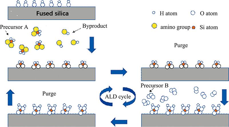
Fig. 1. Schematic diagram of an ALD reaction cycle
The silane precursor A reacts with hydroxyl groups on the surface of fused silica, and the inert gas purges excess precursors and by-products; then the oxidation precursor B reacts with the surface and purges again
The silane precursor A reacts with hydroxyl groups on the surface of fused silica, and the inert gas purges excess precursors and by-products; then the oxidation precursor B reacts with the surface and purges again
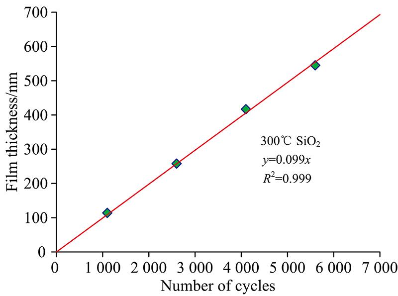
Fig. 2. Thickness of ALD film versus growth cycle, the growth rate of SiO2is about 0.1 nm·cycle-1
Fig. 3. Deposition rate versus deposition temperature
In the experimental temperature range, the deposition rate increases with increasing temperature of substrate
In the experimental temperature range, the deposition rate increases with increasing temperature of substrate
Fig. 4. XRD of SiO2 films deposited by ALD. The SiO2 films are amorphous at different temperatures
Fig. 5. Sample surface roughness
(a): Fused silica substrate, 1.88 nm; (b): 275 ℃, 0.89 nm; (c): 300 ℃, 0.76 nm; (d): 325 ℃, 0.88 nm; (e): 350 ℃, 1.67 nm
(a): Fused silica substrate, 1.88 nm; (b): 275 ℃, 0.89 nm; (c): 300 ℃, 0.76 nm; (d): 325 ℃, 0.88 nm; (e): 350 ℃, 1.67 nm
Fig. 6. Ultraviolet-visible-near infrared transmission spectrum. SiO2 films at different temperatures have no obvious effect on the spectral transmittance of the film
Fig. 7. Fourier transform infrared spectroscopy (FTIR)
(a): 400~1 500 cm-1; (b): near 480 cm-1; (c): near 780 cm-1; (d): near 1 120 cm-1; (e): 2 000~4 000 cm-1
(a): 400~1 500 cm-1; (b): near 480 cm-1; (c): near 780 cm-1; (d): near 1 120 cm-1; (e): 2 000~4 000 cm-1
Fig. 8. (a) Fluorescence spectra curve and (b) peak fluorescence intensity of ALD films at different temperatures. SiO2 films deposited at higher temperatures are closer to the characteristics of fused silica substrate
Fig. 9. (a) Damage probability curve and (b) zero probability damage threshold of ALD films at different temperatures. The damage performances after ALD coating are lower than that of the initial substrate
| |||||||||||||||||||||||||||||||||||||||||||
Table 1. Thickness uniformity of films deposited by ALD
|
Table 2. Growth rate and refractive index of SiO2 film deposited at different temperatures

Set citation alerts for the article
Please enter your email address
© Copyright 2018-2021 | Chinese Laser Press. All Rights Reserved 沪ICP备15018463号-20