• Chinese Optics Letters
  • Vol. 17, Issue 9, 093102 (2019)
Kui Zhang1、2, Zhengwei Wang1、2, Guodong Chen1、2, Yang Wang1、*, Aijun Zeng1, Jing Zhu1, Syarhei Avakaw3, and Heorgi Tsikhanchuk3
Author Affiliations
  • 1Laboratory of Micro-Nano Optoelectronic Materials and Devices, Key Laboratory of Materials for High-Power Laser, Shanghai Institute of Optics and Fine Mechanics, Chinese Academy of Sciences, Shanghai 201800, China
  • 2Center of Materials Science and Optoelectronics Engineering, University of Chinese Academy of Sciences, Beijing 100049, China
  • 3KBTEM-OMO Joint Stock Company, Minsk 220033, Republic of Belarus
  • show less
    DOI: 10.3788/COL201917.093102 Cite this Article Set citation alerts
    Kui Zhang, Zhengwei Wang, Guodong Chen, Yang Wang, Aijun Zeng, Jing Zhu, Syarhei Avakaw, Heorgi Tsikhanchuk. Te-free SbBi thin film as a laser heat-mode photoresist[J]. Chinese Optics Letters, 2019, 17(9): 093102 Copy Citation Text show less
    Basic characteristics of SbBi thin films. The AFM images of (a) as-deposited and (b) laser-irradiated SbBi thin films; (c) XRD patterns of as-deposited and laser-irradiated SbBi thin films; (d) absorption spectra of as-deposited SbBi thin film sample and glass substrate.
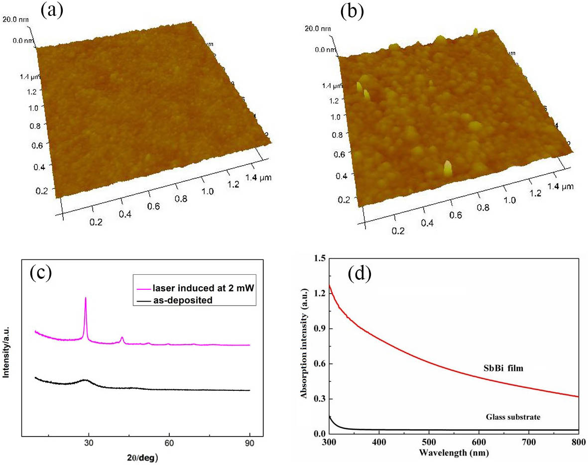
    Fig. 1. Basic characteristics of SbBi thin films. The AFM images of (a) as-deposited and (b) laser-irradiated SbBi thin films; (c) XRD patterns of as-deposited and laser-irradiated SbBi thin films; (d) absorption spectra of as-deposited SbBi thin film sample and glass substrate.
    Comparison of wet-etching selectivity in 17% (NH4)2S solution between as-deposited and laser-irradiated SbBi thin films. The laser irradiation power is fixed at 2 mW.
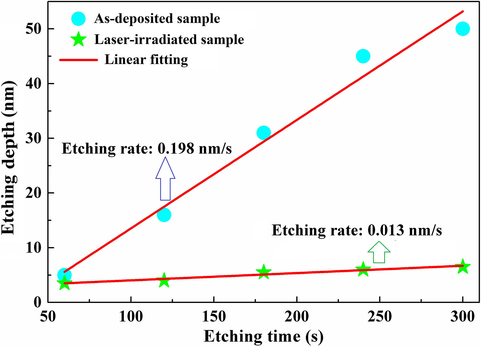
    Fig. 2. Comparison of wet-etching selectivity in 17% (NH4)2S solution between as-deposited and laser-irradiated SbBi thin films. The laser irradiation power is fixed at 2 mW.
    AFM images of fabricated structures on SbBi thin films: (a) line-type patterns without wet-etching; (b) line-type structures after wet-etching for 5 min in 17% (NH4)2S solution; (c) dot-type structures after wet-etching for 5 min in 17% (NH4)2S solution.
    Fig. 3. AFM images of fabricated structures on SbBi thin films: (a) line-type patterns without wet-etching; (b) line-type structures after wet-etching for 5 min in 17% (NH4)2S solution; (c) dot-type structures after wet-etching for 5 min in 17% (NH4)2S solution.
    (a) Principle of preparation of small-period grating structures; (b) AFM image of grating structures with a period of 0.8 μm.
    Fig. 4. (a) Principle of preparation of small-period grating structures; (b) AFM image of grating structures with a period of 0.8 μm.
    Images of complex pattern structures. The original pictures of (a) the Star of David and (b) logo of CAS. The structures fabricated on SbBi thin films: (c) the Star of David and (d) logo of CAS.
    Fig. 5. Images of complex pattern structures. The original pictures of (a) the Star of David and (b) logo of CAS. The structures fabricated on SbBi thin films: (c) the Star of David and (d) logo of CAS.
    Kui Zhang, Zhengwei Wang, Guodong Chen, Yang Wang, Aijun Zeng, Jing Zhu, Syarhei Avakaw, Heorgi Tsikhanchuk. Te-free SbBi thin film as a laser heat-mode photoresist[J]. Chinese Optics Letters, 2019, 17(9): 093102
    Download Citation