
Zhaoxi Chen, Jingwei Yang, Wing-Han Wong, Edwin Yue-Bun Pun, Cheng Wang, "Broadband adiabatic polarization rotator-splitter based on a lithium niobate on insulator platform," Photonics Res. 9, 2319 (2021)
- Photonics Research
- Vol. 9, Issue 12, 2319 (2021)
Abstract
1. INTRODUCTION
Recent years have witnessed the rapid development of photonic devices in the lithium niobate on insulator (LNOI) platform, where strongly confined optical waveguides are formed in a submicrometer lithium niobate (LN) device layer on top of low-index substrates [1–3]. A wide range of high-performance photonic devices have been developed, including low-voltage and high-speed electro-optic modulators [4–6], efficient wavelength conversion devices [7,8], broadband frequency comb sources [9,10], as well as entangled photon pair generators [11,12]. Combining the excellent device performances with the commercial availability of LNOI wafers (up to 6 inches), photonic integrated circuits based on the LNOI platform are becoming a promising cost-effective solution for future optical communications systems in both the classical and quantum domains. Many of these systems make use of the polarization degree of freedom for information encoding and as a result are in need of devices that could efficiently perform tasks like polarization rotation and polarization splitting [13–17]. On the other hand, polarization manipulation devices are also important for processing incoming optical signals that do not possess a pure polarization state (e.g., from non-polarization-maintaining fibers).
A polarization rotator-splitter (PRS) is a promising solution that could address these demands. It is a compact device that can perform two polarization manipulation tasks, i.e., polarization rotation and polarization splitting, in one shot. A typical PRS splits two orthogonally polarized optical signals in the input port and separates them into different output ports while performing a 90° polarization rotation to one of the input signals as is schematically shown in Fig. 1(a). Reversing the input/output ports of a PRS effectively turns it into a polarization rotator-combiner due to reciprocity. Efficient PRSs have been realized in many popular integrated photonic platforms, including silicon (Si) [18–21], silicon nitride (SiN) [22], and indium phosphide (InP) [23]. These PRSs are mainly based on two strategies: mode coupling and mode evolution. The mode-coupling scheme typically features compact device footprints but is relatively narrowband and is more sensitive to fabrication variations [24]. On the other hand, mode-evolution-based PRSs require longer devices to fulfill the adiabatic evolution conditions, while exhibiting much wider operating bandwidths and better fabrication tolerance [21]. Most of these PRSs require a two-step etching process to create mode hybridization with sufficient coupling strength in rib-like waveguide structures [22,25,26]. More recently, computational inverse design methods have also been applied to realize ultracompact polarization manipulation devices in silicon-on-insulator (SOI) platforms [27–29]. In the LNOI platform, a polarization rotator has been demonstrated with plasmonic assisted waveguide structures [30], while PRSs have only been investigated theoretically so far [31–33]. Realization of broadband PRS could greatly expand the device toolbox of the LNOI platform.
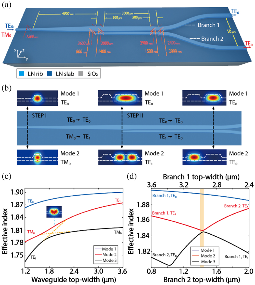
Figure 1.(a) Schematic of the polarization rotator-splitter (PRS). In each taper section, the top widths of Branch 1 (Branch 2) are labeled in red (orange); lengths are labeled in yellow. (b) Optical eigenmode profiles (electric field intensity, viewed from the receiving end) at different locations along the PRS. Top (Mode 1) and bottom (Mode 2) profiles correspond to mode evolutions for
In this work, we design and experimentally demonstrate a PRS in the LNOI platform, based on a two-stage adiabatic mode evolution process. The device fabrication only requires a single etching step, and the resulting rib waveguide geometry is highly compatible with previously reported LNOI devices. The PRS shows a broad operation bandwidth from 1500 to 1630 nm (limited by our laser range), covering the entire telecom C- and L-bands and most of the S-band, with measured polarization crosstalks of
Sign up for Photonics Research TOC. Get the latest issue of Photonics Research delivered right to you!Sign up now
2. DEVICE DESIGN AND OPERATION PRINCIPLE
Figure 1(a) shows the schematic illustration of the on-chip PRS based on air-cladded LNOI waveguides. The PRS splits two input modes, namely, fundamental transverse-electric (
In the polarization rotator (Step I), the LN rib waveguide adiabatically widens from a top width of 1.2 to 3.6 μm via a linear taper, such that the effective index of the second-order TE (
In Step II, an adiabatic coupler is designed to separate the
Figures 2(a) and 2(b) show the numerically simulated electric field evolution along the PRS for
![]()
Figure 2.(a), (b) Simulated electric field intensity evolution along the PRS for (a)
3. DEVICE FABRICATION AND CHARACTERIZATION
We fabricate the designed PRS using a commercial
![]()
Figure 3.Scanning electron microscope (SEM) images of (a) the polarization splitter (Step II) and the output bends, and the zoom-in views of (b) the adiabatic coupler and (c) the output straight waveguide.
We first characterize the polarization splitting and rotation performances of our devices by directly imaging the optical mode profiles at the output facets of the PRS using a measurement setup shown in Fig. 4(a). Continuous-wave (CW) light from a broadband tunable telecom laser (Santec TSL-550, 1500–1630 nm) is launched to the input facet of the PRS through an SMF-28 lensed fiber with a focal spot size of 2 μm (OZ optics). A free-space fiber-bench polarization controller (FFBPC) is used to accurately control the input polarization state. At the output end, we directly image the optical profile using an objective lens focused at the chip facet and an infrared camera (Hamamatsu, C10366). A linear polarizer (LP) is used before the camera to examine the output optical profiles in specific polarization states (TE in the following experiments).
![]()
Figure 4.(a) Experimental setup for output mode characterization. The free-space fiber-bench polarization controller (FFBPC) consists of a quarter-wave plate (QWP), a linear polarizer (LP), and a second QWP. (b) Infrared camera images of the mode profiles at the device output facet in cases of various input polarization states. The top row (i, ii, and iii) shows the output from a device with Step I only (objective lens
Using the direct imaging method, we show that our PRS could efficiently realize the designed polarization-control functions. To separately investigate the mode evolution performance in each section of our PRS, we fabricate and test two types of devices, i.e., devices with Step I only (converting
To further quantitatively characterize the conversion efficiencies and polarization crosstalks of our PRS, we replace the objective lens at the output end with a second lensed fiber to collect the optical signals from a single output port at a time. The output optical powers for
![]()
Figure 5.Measured optical transmission spectra at the PRS output (a) Port 1 and (b) Port 2 in the wavelength range of 1500–1630 nm. Black and red curves correspond to
The measurement results confirm that our PRS design could well cover the entire C- and L-bands and majority of the S-band, limited only by the tuning range of our laser source, thanks to the adiabatic nature of these devices. The PRS performance could in principle be maintained as long as the mode hybridization point exists within the taper structure. Figure 6 shows the waveguide widths at which mode hybridization emerges, as functions of operating wavelength in Step I rotator and Step II splitter, respectively. The pink shades correspond to the actual taper range in Step I (from 1.2 to 3.6 μm) [Fig. 6(a)] and the critical taper range in the slowly tapering middle stage of Step II (Branch 1 tapering from 3.0 to 2.9 μm) [Fig. 6(b)]. The results in Fig. 6 indicate that Step I rotator could efficiently perform
![]()
Figure 6.Simulated mode hybridization points as functions of wavelength in (a) Step I rotator and (b) Step II splitter. The shaded area indicates the actual tapering regions in our device.
4. CONCLUSIONS
In conclusion, we design and experimentally demonstrate an adiabatic PRS based on the LNOI platform, achieved by a single etching step. We show polarization crosstalk of
Acknowledgment
Acknowledgment. We thank Mr. Ke Zhang, Dr. Wenzhao Sun, and Mr. Hanke Feng for their help in device fabrication and SEM imaging, and we thank Dr. Di Zhu for helpful discussions.
References
[1] A. Boes, B. Corcoran, L. Chang, J. Bowers, A. Mitchell. Status and potential of lithium niobate on insulator (LNOI) for photonic integrated circuits. Laser Photon. Rev., 12, 1700256(2018).
[2] D. Zhu, L. Shao, M. Yu, R. Cheng, B. Desiatov, C. J. Xin, Y. Hu, J. Holzgrafe, S. Ghosh, A. Shams-Ansari, E. Puma, N. Sinclair, C. Reimer, M. Zhang, M. Lončar. Integrated photonics on thin-film lithium niobate. Adv. Opt. Photon., 13, 242-352(2021).
[3] J. Lin, F. Bo, Y. Cheng, J. Xu. Advances in on-chip photonic devices based on lithium niobate on insulator. Photon. Res., 8, 1910-1936(2020).
[4] C. Wang, M. Zhang, X. Chen, M. Bertrand, A. Shams-Ansari, S. Chandrasekhar, P. Winzer, M. Loncar. Integrated lithium niobate electro-optic modulators operating at CMOS-compatible voltages. Nature, 562, 101-104(2018).
[5] M. Xu, M. He, H. Zhang, J. Jian, Y. Pan, X. Liu, L. Chen, X. Meng, H. Chen, Z. Li, X. Xiao, S. Yu, S. Yu, X. Cai. High-performance coherent optical modulators based on thin-film lithium niobate platform. Nat. Commun., 11, 3911(2020).
[6] P. Kharel, C. Reimer, K. Luke, L. He, M. Zhang. Breaking voltage–bandwidth limits in integrated lithium niobate modulators using micro-structured electrodes. Optica, 8, 357-363(2021).
[7] C. Wang, C. Langrock, A. Marandi, M. Jankowski, M. Zhang, B. Desiatov, M. M. Fejer, M. Lončar. Ultrahigh-efficiency wavelength conversion in nanophotonic periodically poled lithium niobate waveguides. Optica, 5, 1438-1441(2018).
[8] J. Lu, J. B. Surya, X. Liu, A. W. Bruch, Z. Gong, Y. Xu, H. X. Tang. Periodically poled thin-film lithium niobate microring resonators with a second-harmonic generation efficiency of 250,000%/W. Optica, 6, 1455-1460(2019).
[9] M. Zhang, B. Buscaino, C. Wang, A. Shams-Ansari, C. Reimer, R. Zhu, J. M. Kahn, M. Loncar. Broadband electro-optic frequency comb generation in a lithium niobate microring resonator. Nature, 568, 373-377(2019).
[10] Y. He, Q.-F. Yang, J. Ling, R. Luo, H. Liang, M. Li, B. Shen, H. Wang, K. Vahala, Q. Lin. Self-starting bi-chromatic LiNbO3 soliton microcomb. Optica, 6, 1138-1144(2019).
[11] J. Zhao, C. Ma, M. Rusing, S. Mookherjea. High quality entangled photon pair generation in periodically poled thin-film lithium niobate waveguides. Phys. Rev. Lett., 124, 163603(2020).
[12] B. S. Elkus, K. Abdelsalam, A. Rao, V. Velev, S. Fathpour, P. Kumar, G. S. Kanter. Generation of broadband correlated photon-pairs in short thin-film lithium-niobate waveguides. Opt. Express, 27, 38521-38531(2019).
[13] D. Dai, C. Li, S. Wang, H. Wu, Y. Shi, Z. Wu, S. Gao, T. Dai, H. Yu, H.-K. Tsang. 10-channel mode (de)multiplexer with dual polarizations. Laser Photon. Rev., 12, 1700109(2018).
[14] C. Ma, W. D. Sacher, Z. Tang, J. C. Mikkelsen, Y. Yang, F. Xu, T. Thiessen, H.-K. Lo, J. K. S. Poon. Silicon photonic transmitter for polarization-encoded quantum key distribution. Optica, 3, 1274-1278(2016).
[15] H. P. Chung, C. H. Lee, K. H. Huang, S. L. Yang, K. Wang, A. S. Solntsev, A. A. Sukhorukov, F. Setzpfandt, Y. H. Chen. Broadband on-chip polarization mode splitters in lithium niobate integrated adiabatic couplers. Opt. Express, 27, 1632-1645(2019).
[16] C. Sun, Y. Yu, Y. Ding, Z. Li, W. Qi, X. Zhang. Integrated mode-transparent polarization beam splitter supporting thirteen data channels. Photon. Res., 8, 978-985(2020).
[17] D. González-Andrade, C. Lafforgue, E. Durán-Valdeiglesias, X. Le Roux, M. Berciano, E. Cassan, D. Marris-Morini, A. V. Velasco, P. Cheben, L. Vivien. Polarization-and wavelength-agnostic nanophotonic beam splitter. Sci. Rep., 9, 3604(2019).
[18] D. Dai, J. E. Bowers. Novel concept for ultracompact polarization splitter-rotator based on silicon nanowires. Opt. Express, 19, 10940-10949(2011).
[19] D. Dai, Y. Tang, J. E. Bowers. Mode conversion in tapered submicron silicon ridge optical waveguides. Opt. Express, 20, 13425-13439(2012).
[20] D. Dai, L. Liu, S. Gao, D.-X. Xu, S. He. Polarization management for silicon photonic integrated circuits. Laser Photon. Rev., 7, 303-328(2013).
[21] W. D. Sacher, T. Barwicz, B. J. Taylor, J. K. Poon. Polarization rotator-splitters in standard active silicon photonics platforms. Opt. Express, 22, 3777-3786(2014).
[22] W. D. Sacher, Y. Huang, L. Ding, T. Barwicz, J. C. Mikkelsen, B. J. Taylor, G. Q. Lo, J. K. Poon. Polarization rotator-splitters and controllers in a Si3N4-on-SOI integrated photonics platform. Opt. Express, 22, 11167-11174(2014).
[23] C.-J. Chung, J. Midkiff, K. M. Yoo, A. Rostamian, J. Guo, R. T. Chen, S. Chakravarty. InP-based polarization rotator-splitter for mid-infrared photonic integration circuits. AIP Adv., 9, 015303(2019).
[24] H. Guan, A. Novack, M. Streshinsky, R. Shi, Q. Fang, A. E. Lim, G. Q. Lo, T. Baehr-Jones, M. Hochberg. CMOS-compatible highly efficient polarization splitter and rotator based on a double-etched directional coupler. Opt. Express, 22, 2489-2496(2014).
[25] Y. Xiong, D. X. Xu, J. H. Schmid, P. Cheben, S. Janz, W. N. Ye. Fabrication tolerant and broadband polarization splitter and rotator based on a taper-etched directional coupler. Opt. Express, 22, 17458-17465(2014).
[26] K. Tan, Y. Huang, G. Q. Lo, C. Lee, C. Yu. Compact highly-efficient polarization splitter and rotator based on 90 degrees bends. Opt. Express, 24, 14506-14512(2016).
[27] S. Molesky, Z. Lin, A. Y. Piggott, W. Jin, J. Vucković, A. W. Rodriguez. Inverse design in nanophotonics. Nat. Photonics, 12, 659-670(2018).
[28] W. Chang, S. Xu, M. Cheng, D. Liu, M. Zhang. Inverse design of a single-step-etched ultracompact silicon polarization rotator. Opt. Express, 28, 28343-28351(2020).
[29] B. Shen, P. Wang, R. Polson, R. Menon. An integrated-nanophotonics polarization beamsplitter with 2.4 × 2.4 μm2 footprint. Nat. Photonics, 9, 378-382(2015).
[30] Y. Zhao, W. Yu, S. Dai, J. Li, T. Lin, M. Li, J. Liu. Compact lithium-niobate-on-insulator polarization rotator based on asymmetric hybrid plasmonics waveguide. IEEE Photon. J., 13, 4800105(2021).
[31] Z. Y. Chen, Y. Pan, X. Y. Liu, H. T. Lin, X. M. Zhong, X. L. Cai. Single-step etching polarization splitter-rotator based on lithium niobate ridge waveguide. Asia Communications and Photonics Conference, M4A-285(2019).
[32] L. Zhang, L. Zhang, X. Fu, L. Yang. Compact, broadband and low-loss polarization beam splitter on lithium-niobate-on-insulator using a silicon nanowire assisted waveguide. IEEE Photon. J., 12, 6601906(2020).
[33] A. Pan, C. Hu, C. Zeng, J. Xia. Fundamental mode hybridization in a thin film lithium niobate ridge waveguide. Opt. Express, 27, 35659-35669(2019).
[34] K. Zhang, Z. Chen, H. Feng, W. H. Wong, E. Y. B. Pun, C. Wang. High-
[35] Z. Chen, Q. Xu, K. Zhang, W. H. Wong, D. L. Zhang, E. Y. B. Pun, C. Wang. Efficient erbium-doped thin-film lithium niobate waveguide amplifiers. Opt. Lett., 46, 1161-1164(2021).
[36] M. Zhang, C. Wang, R. Cheng, A. Shams-Ansari, M. Lončar. Monolithic ultra-high-


Set citation alerts for the article
Please enter your email address

© Copyright 2018-2021 | Chinese Laser Press. All Rights Reserved 沪ICP备15018463号-20