• Chinese Optics Letters
  • Vol. 20, Issue 7, 071403 (2022)
Jing Liu1,2,*, Mingjin Wang1, Yufei Wang1,2,3,4, Xuyan Zhou1..., Ting Fu1,2, Aiyi Qi1,3, Hongwei Qu1,2,3,4, Xiaoxu Xing1,2 and Wanhua Zheng1,2,3,4,5,**|Show fewer author(s)
Author Affiliations
  • 1Laboratory of Solid-State Optoelectronics Information Technology, Institute of Semiconductors, Chinese Academy of Sciences, Beijing 100083, China
  • 2Center of Materials Science and Optoelectronics Engineering, University of Chinese Academy of Sciences, Beijing 100049, China
  • 3State Key Laboratory on Integrated Optoelectronics, Institute of Semiconductors, Chinese Academy of Sciences, Beijing 100083, China
  • 4College of Future Technology, University of Chinese Academy of Sciences, Beijing 101408, China
  • 5School of Electronic, Electrical and Communication Engineering, University of Chinese Academy of Sciences, Beijing 100049, China
  • show less
    DOI: 10.3788/COL202220.071403 Cite this Article Set citation alerts
    Jing Liu, Mingjin Wang, Yufei Wang, Xuyan Zhou, Ting Fu, Aiyi Qi, Hongwei Qu, Xiaoxu Xing, Wanhua Zheng, "High peak power density and low mechanical stress photonic-band-crystal diode laser array based on non-soldered packaging technology," Chin. Opt. Lett. 20, 071403 (2022) Copy Citation Text show less
    Schematic of a single MCC diode laser.
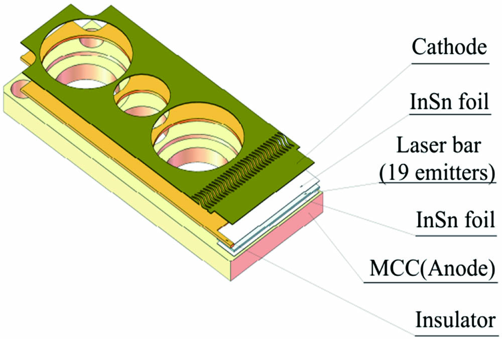
    Fig. 1. Schematic of a single MCC diode laser.
    Schematic of the vertical diode laser array.
    Fig. 2. Schematic of the vertical diode laser array.
    Schematic of a single PBC laser emitter.
    Fig. 3. Schematic of a single PBC laser emitter.
    Far-field incoherent irradiance distribution of the two diode laser arrays. (a) Irradiance distribution of the PBC diode laser array. (b) Irradiance distribution of the conventional diode laser array.
    Fig. 4. Far-field incoherent irradiance distribution of the two diode laser arrays. (a) Irradiance distribution of the PBC diode laser array. (b) Irradiance distribution of the conventional diode laser array.
    Simulation model of the PBC laser bar.
    Fig. 5. Simulation model of the PBC laser bar.
    Stress distribution of the two PBC diode laser bars. (a) Stress distribution of the bar with indium soldered. (b) Stress distribution of the bar with non-soldered.
    Fig. 6. Stress distribution of the two PBC diode laser bars. (a) Stress distribution of the bar with indium soldered. (b) Stress distribution of the bar with non-soldered.
    Deformation distribution of the two PBC diode laser bars. (a) Deformation distribution of the bar with indium soldered. (b) Deformation distribution of the bar with non-soldered.
    Fig. 7. Deformation distribution of the two PBC diode laser bars. (a) Deformation distribution of the bar with indium soldered. (b) Deformation distribution of the bar with non-soldered.
    Temperature distribution of the two PBC diode laser bars. (a) Temperature distribution of the bar with indium soldered. (b) Temperature distribution of the bar with non-soldered.
    Fig. 8. Temperature distribution of the two PBC diode laser bars. (a) Temperature distribution of the bar with indium soldered. (b) Temperature distribution of the bar with non-soldered.
    Light spots in free transmission of the two diode laser bars. (a) Light spot of the conventional bar. (b) Light spot of the PBC bar.
    Fig. 9. Light spots in free transmission of the two diode laser bars. (a) Light spot of the conventional bar. (b) Light spot of the PBC bar.
    (a) PBC diode laser array with two non-soldered bars. (b) P and N sides contact.
    Fig. 10. (a) PBC diode laser array with two non-soldered bars. (b) P and N sides contact.
    (a) Power, (b) slope efficiency, and (c) wavelength of the PBC diode laser arrays with non-soldered and indium soldered.
    Fig. 11. (a) Power, (b) slope efficiency, and (c) wavelength of the PBC diode laser arrays with non-soldered and indium soldered.
    “Smile” of the PBC diode laser array with non-soldered. (a) The “smile.” (b) The optimized “smile.”
    Fig. 12. “Smile” of the PBC diode laser array with non-soldered. (a) The “smile.” (b) The optimized “smile.”
    ParametersPBC Laser DiodeConventional Diode Laser
    Fast axis divergence (FWHM)15°36°
    Slow axis divergence (FWHM)
    Emitter width in the slow axis200 µm200 µm
    Number of emitters1919
    Emitter pitch500 µm500 µm
    Table 1. Parameters of PBC and Conventional Laser Bar
    MaterialDensity (kg·m3)CTE (106K1)Thermal Conductivity (W·m1·K1)Poisson’s RatioHeat Capacity (J·kg1·K1)Young’s Modulus (Pa)
    Cu890016.53980.363951.3×1011
    GaAs53306.4440.303257.5×109
    In73103381.60.452301.1×1010
    InSn730020340.452301.6×1010
    Table 2. Parameters of Material Performance
    Jing Liu, Mingjin Wang, Yufei Wang, Xuyan Zhou, Ting Fu, Aiyi Qi, Hongwei Qu, Xiaoxu Xing, Wanhua Zheng, "High peak power density and low mechanical stress photonic-band-crystal diode laser array based on non-soldered packaging technology," Chin. Opt. Lett. 20, 071403 (2022)
    Download Citation