
Xiao-Juan Liang, Yu Cao, Hong-Kun Cai, Jian Su, Jian Ni, Juan Li, Jian-Jun Zhang. Simulation and architectural design for Schottky structure perovskite solar cells [J]. Acta Physica Sinica, 2020, 69(5): 057901-1
- Acta Physica Sinica
- Vol. 69, Issue 5, 057901-1 (2020)
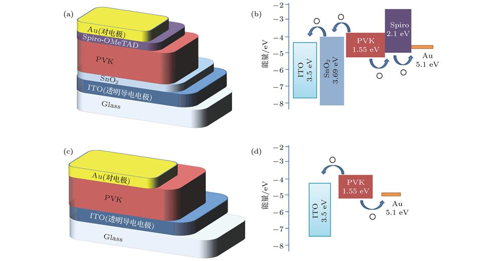
Fig. 1. Schematic and energy-level diagram of each functional layers of solar cells: (a), (b) planar heterojunction solar cell structure; (c), (d) schottky solar cell structure.
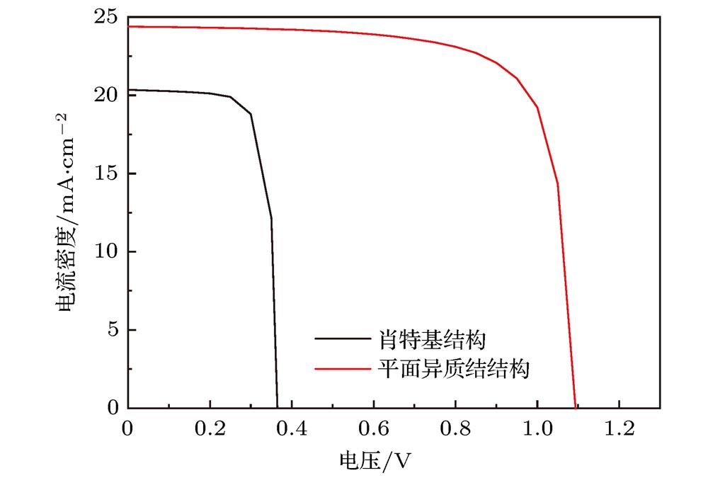
Fig. 2. J -V characteristics of pin solar cell structure and Schottky solar cell structure.
Fig. 3. Energy band diagram and schematic diagram of photogenerated electron and hole transport: (a) Pin solar cell structure; (b) Schottky solar cell structure.
Fig. 4. Schottky solar cells with different front electrode: (a) Energy band structure; (b) carrier recombination rate distribution; (c) electric field distribution; (d) free electrons concentration distribution; (e) quantum efficiency; (f) J -V characteristic.
Fig. 5. Schottky solar cells with different back electrode: (a) Energy band structure; (b) carrier recombination rate distribution; (c) electric field distribution; (d) free electrons concentration distribution; (e) quantum efficiency; (f) J -V characteristic.
Fig. 6. Output trends under different acceptor doping concentration: (a) V oc and J sc; (b) FF and PCE.
Fig. 7. Output trends under different donor doping concentration: (a) V oc and J sc; (b) FF and PCE.
Fig. 8. Output trends under J -V characteristics of Schottky solar cells with and without defect states: (a)J -V characteristic; (b) quantum efficiency; (c) free electrons concentration distribution; (d) free holes concentration distribution.
Fig. 9. Output trends under different thickness of absorbing layer: (a) V oc and J sc; (b) FF and PCE.
|
Table 1.
Material parameters of the Schottky solar cells.
模型中使用的材料参数
|
Table 2.
Photovoltaic performance parameters of the pin solar cell structure and Schottky solar cell structure.
平面异质结结构和肖特基钙钛矿太阳电池光伏性能参数
|
|
Table 4.
Photovoltaic performance parameters of Schottky solar cells with different front electrode work function.
透明导电电极功函数的不同肖特基钙钛矿太阳电池光伏性能参数
|
Table 5.
Photovoltaic performances of Schottky solar cells with different back electrode work function.
对电极功函数不同肖特基钙钛矿太阳电池光伏性能
|
Table 6.
Photovoltaic performance of Schottky solar cells with and without defect states.
有无缺陷的肖特基钙钛矿太阳电池的光电特性

Set citation alerts for the article
Please enter your email address
© Copyright 2018-2021 | Chinese Laser Press. All Rights Reserved 沪ICP备15018463号-20