Abstract
The development of semiconductors is always accompanied by the progress in controllable doping techniques. Taking AlGaN-based ultraviolet (UV) emitters as an example, despite a peak wall-plug efficiency of 15.3% at the wavelength of 275 nm, there is still a huge gap in comparison with GaN-based visible light-emitting diodes (LEDs), mainly attributed to the inefficient doping of AlGaN with increase of the Al composition. First, p-doping of Al-rich AlGaN is a long-standing challenge and the low hole concentration seriously restricts the carrier injection efficiency. Although p-GaN cladding layers are widely adopted as a compromise, the high injection barrier of holes as well as the inevitable loss of light extraction cannot be neglected. While in terms of n-doping the main issue is the degradation of the electrical property when the Al composition exceeds 80%, resulting in a low electrical efficiency in sub-250 nm UV-LEDs. This review summarizes the recent advances and outlines the major challenges in the efficient doping of Al-rich AlGaN, meanwhile the corresponding approaches pursued to overcome the doping issues are discussed in detail.Introduction
Semiconductors stand at the heart of modern electronics and optoelectronics, largely thanks to the development of controllable doping techniques. The realization of p−n and p−i−n junctions lays the foundation for a series of applications, such as light-emitting diodes (LEDs)[1, 2], laser diodes (LDs)[3, 4] and photodetectors[5, 6]. In other words, the performance improvement of these devices hinges on having both high-quality n- and p-type doping. Taking GaN-based visible LEDs as an example, one of the milestones is the breakthrough in creating a p-doped GaN layer[7, 8], which is a vital part of the contributions of I. Akasaki, H. Amano and S. Nakamura for winning the 2014 Nobel Prize in Physics.
Over the past two decades, one of the predominant development directions for Ⅲ-nitride semiconductors aims at shorter-wavelength optoelectronics, i.e. AlGaN-based ultraviolet (UV) emitters[9−13], which have attracted much attention owing to the advantages of long lifetime, potential high efficiency, environmentally friendly, and portability in comparison with the conventional mercury UV lamps. As of 2022, the total market for UV light source reached US$ ~1.8 B with a compound annual growth rate (CARG) of 17.8%, wherein AlGaN-based UV-LEDs account for more than half of the annual increase[14].
By varying the Al composition, AlGaN-based UV-LEDs (210−360 nm) can cover almost the entire UV spectral range. The emission wavelength directly determines the applications. In general, UVA (320−400 nm) and UVB (280−320 nm) light sources are employed for UV curing and phototherapy, respectively. More importantly, the highest volume UV application is disinfection and sterilization in the UVC band (100−280 nm). Based on Al-rich AlGaN (Al composition higher than 50%), the solid state AlGaN-based UVC-LEDs show great potential and they are expected to eventually substitute for the mercury lamps, in accordance with the Minamata Convention[15].
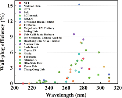
The wall-plug efficiency (WPE) is the most commonly used figure of merit to assess the performance of UV-LEDs, which strongly depends on the emission wavelength as shown in Fig. 1[16−47]. Although a peak WPE of 15.3% has been achieved for UV-LEDs at 275 nm[16], there is still a huge gap in comparison with GaN-based visible LEDs. Moreover, there is a sharp drop of WPE in sub-250 nm UV-LEDs, as well as a significant dip across the UVB band. Hence, it is quite necessary to understand the performance limitations of UV-LEDs, especially the restriction from the doping issues with increase of the Al composition.
![(Color online) State of the art of UV-LEDs in the wavelength of 210−320 nm. The wall-plug efficiency values are plotted as reported or calculated from reported voltage, current, and light output power. Data obtained from Refs. [9, 16−47].](/Images/icon/loading.gif)
Figure 1.(Color online) State of the art of UV-LEDs in the wavelength of 210−320 nm. The wall-plug efficiency values are plotted as reported or calculated from reported voltage, current, and light output power. Data obtained from Refs. [9, 16−47].
The WPE is defined as the ratio of the light output power (LOP) and the electric input power, and it can be subdivided into the efficiency of different processes within the devices. Generally, these processes can fall into two categories, i.e. the opto-related part and the electrical part. The former consists of the radiative efficiency (RE) and light extraction efficiency (LEE), describing the likelihood of UV photon generation by the radiative recombination, as well as the subsequent escape from the chips, respectively. While the latter includes the carrier injection efficiency (CIE) and the electrical efficiency, both of which are the foundation of UV-LEDs as a typical p−i−n structure. On the one hand, the electron and hole concentration in the cladding layers directly determines the CIE (Fig. 2(a)), as well as the contact property of electrodes (relevant to the electrical efficiency). On the other hand, the current spreading in the cladding layers is largely related to the series resistance and operating voltage of devices (relevant to the electrical efficiency), especially in the geometry of flip-chip configuration as shown in Fig. 2(b)[12].
Figure 2.(Color online) (a) Schematic band diagram and carrier injection in AlGaN-based UV-LEDs. (b) Equivalent circuit diagram for AlGaN-based UV-LEDs with the flip-chip configuration. The voltage drops are estimated under the current densities of 50−100 A/cm2 [12].
Moreover, doping in the cladding layers indirectly influences the LEE in UV-LEDs. Specifically, owing to the lack of a thorough solution for p-type doping in Al-rich AlGaN, a thick p-GaN layer is widely adopted as a substitute[25, 27, 33, 37, 39, 41, 43]. Hence, the vast majority of the UV light emitted towards the p-region is absorbed, restricting the increase of LEE as well as WPE. According to the peak WPE of 15.3% by Nikkiso Giken Co., Ltd., a combination of a transparent Al-rich p-AlGaN cladding layer, a thin p-GaN contact layer and a reflective p-electrode are optimum to significantly improve the device performance[16], which is, however, based on the realization of efficient p-doping in Al-rich AlGaN.
This review focuses on the recent progress in efficient doping of AlGaN with Al composition higher than 50%, which is applicable to sub-300 nm UV-LEDs. In this work, we summarize the recent advances and outline the major challenges in the efficient doping of Al-rich AlGaN. The corresponding approaches pursued to overcome the doping issues are discussed in detail.
Progress of n-doped Al-rich AlGaN
Al-rich AlGaN with Al composition higher than 50% suffers from a doping asymmetry issue, i.e. realization of efficient n-type doping is comparatively easier than p-type one. The state of the art of n-doped Al-rich AlGaN has been summarized in Fig. 3, where the conductivity and electron concentration in n-AlGaN with Al composition lower than 80% reach the order of 102 S/cm and 1019 cm−3, respectively. While the Al composition exceeds 80%, a sharp degradation of electrical property is observed, partially resulting in the extremely low WPE in sub-250 nm UV-LEDs.
Figure 3.(Color online) State of the art of (a) conductivity and (b) electron concentration in n-doped Al-rich AlGaN. Data obtained from Refs. [50, 52−65, 70, 74−76].
The electrical property of n-AlGaN is generally related to the compensating defects, e.g. the cation vacancy and DX centers. Hence a series of point defect control schemes for n-AlGaN epitaxy have been proposed, not only by metal−organic chemical vapor deposition (MOCVD) but also by molecular beam epitaxy (MBE) and magnetron sputtering deposition.
n-AlGaN with Al composition lower than 80%
Silicon (Si) is the most common dopant for n-doping, which shows a relatively low activation energy in Ⅲ-nitrides, i.e. a constant at around 15 meV in AlGaN with Al composition lower than 80%[48]. Hence the key to realize high conductivity and electron concentration is to reduce the compensation by defects, including the cation vacancy complexes with Si (VⅢ-nSi) as well as carbon on nitrogen site (CN). Both defects can be suppressed by optimizing the growth conditions of MOCVD, e.g. growth temperature, Ⅴ/Ⅲ ratio and growth rate. In terms of VⅢ-nSi, a low growth temperature, low Ⅴ/Ⅲ ratio and slow growth rate are conducive to increase the formation energy (Fig. 4(a))[49]; while for CN, the requirements are exactly the opposite[50, 51]. Therefore, a trade-off of the growth conditions is essential for efficient n-doping of Al-rich AlGaN, as shown in Fig. 4.
Figure 4.(Color online) Theoretical formation energy change of (a) VⅢ and (b) CN as a function of Ⅴ/Ⅲ ratio and growth rate (proportional to the metalorganic flow)[52]. Experimental trade-off of the (c) growth temperature and (d) Ⅴ/Ⅲ ratio to suppress the formation of VⅢ-nSi and CN[53].
A typical characteristic of the optimized growth conditions is that the growth temperature is relatively low, especially with regard to the epitaxial kinetics of Al-rich AlGaN. Washiyama et al. reported a conductivity of 160 S/cm with an electron concentration of 3 × 1019 cm−3 in n-Al0.7Ga0.3N grown on a single crystal AlN substrate, where the growth temperature was reduced to 1000 °C[52]. Similarly, Nagata et al. realized a conductivity of 152 S/cm in n-Al0.62Ga0.38N with the optimized growth temperature and Ⅴ/Ⅲ ratio being 1040 °C and 1600, respectively[53]. Yang et al. achieved an impressive electrical property with a maximum conductivity of 200 S/cm in n-Al0.57Ga0.43N at the growth temperature of 1040 °C[54]. Studies at University of California Santa Barbara proposed an indium-involved growth approach for n-AlGaN, leading to a conductivity of 133 S/cm in Al0.65Ga0.35N grown at 1050 °C[55]. Additionally, a much lower growth temperature of 920 °C was adopted in the In−Si co-doping method proposed by Cantu et al., where a conductivity of 90 S/cm was realized with an electron concentration of 2.5 × 1019 cm−3 in n-Al0.65Ga0.35N[56].
It is worth noting that although the relatively low growth temperature (lower than 1050 °C) is beneficial to the electrical property, it is unfavorable for the two-dimensional growth of Al-rich AlGaN, hence resulting in the rough surface morphology. Studies at Peking University indicated that the upper-bound growth rate for the smooth surface of n-Al0.65Ga0.35N is around 0.65 μm/h at 1100 °C on conventional sapphire with a miscut angle of 0.2°[57]. It is convinced that the critical rate would further decrease at a lower temperature to pursue better electrical properties in n-AlGaN. This growth rate can hardly meet the requirements for mass production of UV-LEDs, where the thickness of n-AlGaN cladding layer reaches 1.5 μm or even thicker. Hence, we regulated the surface kinetics of AlGaN by shortening the terrace width, which achieved a growth window allowing a higher rate as well as a lower temperature. Specifically, on sapphire with a miscut angle of 0.5°, a growth rate of 2.3 μm/h was realized at 1050 °C for n-Al0.55Ga0.45N with typical step-terrace morphology; meanwhile, a conductivity of 102.8 S/cm was obtained at this appropriate low temperature[58].
In addition to the growth conditions, other factors can affect the compensating defects. Studies at North Carolina State University showed the “knee behavior” by controlling the incorporation of Si dopants into AlGaN. The conductivity and electron concentration increased first and reached a peak at the Si concentration of about 1.5 × 1019 cm−3 as shown in Fig. 5, while higher Si doping levels degraded the electrical property of AlGaN, which was attributed to the increased concentration of VⅢ-nSi as the self-compensating defects[59]. Zollner et al. demonstrated that an extremely reduced Ⅴ/Ⅲ ratio allowed a higher Si concentration (more than 3 × 1019 cm−3) before the degradation of electrical property, where a maximum conductivity of 250 S/cm was realized in n-Al0.65Ga0.35N with a Ⅴ/Ⅲ ratio of 10[60]. The recent studies at the University of Tokyo provided an alternative route to address this issue, where heavily Si-doped AlGaN was grown by magnetron sputtering deposition instead of the conventional MOCVD. The VⅢ-nSi defects were nearly negligible, even at the Si concentration of more than 1020 cm−3, and a record high conductivity of 400 S/cm was realized with an electron concentration of 1.2 × 1020 cm−3 in n-Al0.6Ga0.4N[61].
Figure 5.(Color online) (a) Conductivity and (b) electron concentration as a function of Si concentration in n-Al0.7Ga0.3N[59].
Besides, MBE may be conducive to the electrical property of n-AlGaN because the ultra-high vacuum chamber and high purity sources could significantly reduce the incorporation of self-compensating impurities, in particular the C impurity. Borisov et al. grew n-AlGaN by MBE, where the electron concentration in n-Al0.6Ga0.4N and n-Al0.86Ga0.14N reached 2 × 10¹⁹ and 7 × 1018 cm−3, respectively. SIMS measurements showed that the C concentration was below 1 × 1017 cm−3 in both samples[62]. Similarly, studies at Cornell University realized a conductivity of 133 S/cm with an electron concentration of 3 × 1019 cm−3 in n-Al0.6Ga0.4N grown on a single crystal AlN substrate by MBE[63]. The subsequent application of these methods in UV-LEDs, e.g. the combination of magnetron sputtering/MBE (n-cladding layer) and MOCVD (active region and p-cladding layer), is worth pursuing.
n-Al(Ga)N with Al composition higher than 80%
When the Al composition exceeds 80%, a rapid decrease of conductivity in n-AlGaN (including n-AlN) has been widely reported[64, 65]. In other words, the activation energy of Si sharply increases, as shown in Fig. 6(a)[48, 66, 67], even up to as high as 282 meV in n-AlN[9]. The degradation of the electrical property drastically decreases the electrical efficiency and WPE in sub-250 nm UV-LEDs, which has attracted much attention because it is harmless to exposed human tissues[68, 69].
Figure 6.(Color online) (a) The activation energy of Si in Al-rich AlGaN with Al composition higher than 80%[66]. (b) Configuration coordinate diagram of the DX center in Si-doped Al(Ga)N[74].
Some studies attributed the degradation to the compensation by O-related defects, e.g. O-DX or VⅢ-nON[70, 71]. In addition, studies have demonstrated that Si transformed from a shallow donor to a stable DX center as the Al composition beyond 80%, which acted as a stable and deep charge trapping center[72, 73]. For Si-doped AlGaN, it is believed that the DX center is formed due to a bond-rupturing displacement of Si atoms or the nearest-neighbor Al/Ga atoms in the wurtzite lattice[74]. Fig. 6(b) shows the configuration coordinate diagram of the DX center, where the parabolas labeled Ud, UDX0 and UDX−1 represent the energy for electrons in the conduction band, the metastable DX0 state and stable charged DX−1 state, respectively. The net energy difference (EA) between the substitutional donor and the DX center determines the occupation of the two levels as well as the electrical property of Si-doped AlGaN. For AlGaN with Al composition higher than 80%, this energy difference EA significantly increases, which makes it difficult to thermally ionize Si donors, suggesting a drastic decrease of the effective free electron concentration.
Deviation from the thermal equilibrium may be used to maintain the Si dopant in the shallow state in AlGaN with Al composition higher than 80%. Breckenridge et al. explored an approach of non-equilibrium doping consisting of Si ion implantation and a recovery annealing process, where the n-type conductivity and electron concentration exceeds 1 S/cm and 5 × 1018 cm−3 in AlN[75]. Similarly, Bagheri et al. reported a result of Ge implantation in n-AlN, realizing a conductivity of 0.3 S/cm[76]. MBE is an alternative method to obtain n-doped AlGaN far from equilibrium. Studies at Georgia Institute of Technology achieved an electron concentration of 1018 cm−3 in AlN grown by metal modulated epitaxy in MBE, and a record high conductivity of 43.7 S/cm was obtained[77].
Progress of p-doped Al-rich AlGaN
Challenges to achieve efficient p-doping
As mentioned earlier, p-doping of Al-rich AlGaN has been an enormous challenge. Zhang et al. showed the “doping limit rule” in semiconductors, where the valence band of AlN was quite far from the p-like pinning energy level[78]. In other words, the low hole concentration in Al-rich AlGaN is an intrinsic characteristic. Great efforts have been devoted to p-doping of Al-rich AlGaN, and the major challenges include:
(1) Exceptionally high activation energy of acceptors. Although magnesium (Mg) is a relatively successful p-type dopant, its activation energy increases from 170 meV in GaN to as high as 510 meV in AlN (Fig. 7(a))[9, 79−87], resulting in an extremely low activation efficiency of Mg in Al-rich AlGaN.
Figure 7.(Color online) (a) Activation energy of Mg in dependence of Al composition in AlGaN. Data obtained from Refs. [9, 79−87]. (b) Formation enthalpies of MgGa/MgAl as a function of Al composition in bulk AlGaN under N-rich growth condition[88].
(2) Low solubility of Mg in Al-rich AlGaN. Theoretical calculations indicated that the solubility of Mg as a substitute for Ga or Al in bulk AlGaN was quite limited owing to the positive and large formation enthalpies (Fig. 7(b))[88]. The function of formation enthalpy on the solubility of Mg could be expressed as in the following equation:
where C was the equilibrium Mg solubility, Nsites was the number of lattice points that could be occupied by Mg atoms, ΔHf was the formation enthalpy. As the Al composition increased, both the formation enthalpies of MgAl and MgGa monotonically increased as shown in Fig. 7(b), suggesting low solubility of Mg in Al-rich AlGaN.
(3) Compensation arising from the donor defects and/or related complexes. The nitrogen vacancy (VN), in particular VN3+, is believed to be the main compensating defects in Mg-doped AlGaN[89−91]. The formation of the compensating defects should be suppressed to increase the hole concentration in Al-rich AlGaN.
On account of these three factors, the hole concentration in p-doped Al-rich AlGaN is terribly low and far from satisfying the demand of efficient carrier injection. Hence, a number of targeted approaches have been proposed as shown below.
Approaches to lower the activation energy
Over the past two decades, research has focused on the reduction of the activation energy of Mg and a series of approaches have been put forward. Superlattice (SL) doping is one of the commonly used methods, where the band bending caused by polarization modulates the activating path, and hence lowers the activation energy, as shown in Fig. 8(a)[92]. Ebata et al. adopted 1.3 nm AlN/4 nm Al0.75Ga0.25N SLs to achieve a small activation energy of 40−67 meV, and a hole concentration of 1 × 1018 cm−3 was obtained[93]. Similarly, studies at University of California Santa Barbara realized a maximum hole concentration of 2.1 × 1019 cm−3 in 0.67 nm Al0.95Ga0.05N/0.67 nm Al0.05Ga0.95N and 1.7 nm Al0.8Ga0.2N/1.7 nm Al0.2Ga0.8N SLs[94].
Figure 8.(Color online) (a) Schematic illustration of valence band for p-type superlattice (SL) doping[92]. (b) The vertical miniband transport of holes in Al0.63Ga0.37N/Al0.46Ga0.54N SLs with a constant barrier thickness of 0.75 nm[96].
Although SL doping can effectively lower the activation energy, the vertical hole transport is usually blocked by the barriers, which restricts the effective hole injection into the active region, and consequently the short-period SLs (SPSLs) with thin barriers have been pursued. Simon et al. grew p-type short-period 0.6 nm AlN/1.4 nm GaN SLs by MBE, which showed better vertical transport than those with thicker AlN[95]. Recently, we proposed a desorption-tailoring strategy to assemble Al0.63Ga0.37N/Al0.46Ga0.54N SPSLs with a constant ultrathin barrier thickness of 0.75 nm, where the vertical miniband transport of holes was experimentally verified according to the feature of the negative differential resistance, as shown in Fig. 8(b)[96]. Moreover, as a derivative of the SL doping, the quantum-dot (QD) doping in Al-rich AlGaN was adopted by Jiang et al. The modulation of the valance band in GaN QDs has been verified, leading to a low activation energy of 21 meV in AlGaN with an Al composition of 60%[97].
In addition to the SL doping, the polarization-induced doping provides an alternate route to increase the hole concentration, as proposed by Simon et al[79]. The Al compositional grading and the corresponding polarization-induced negative sheet charge at the heterointerfaces are the core of this method (Fig. 9(a)). Hence, the directions of spontaneous and piezoelectric polarizations should first be clarified[98], in particular for Al-polar AlGaN/AlN as adopted in UV-LEDs. As shown in Fig. 9(b), the spontaneous and piezoelectric polarizations are along the same direction in N-polar AlGaN/GaN, which suggests that this is the optimal demo structure to verify the feasibility of this method. While for Al-polar AlGaN/AlN they are along the opposite direction and partially counteracted, resulting in a relatively low polarization-induced net sheet charge. A detailed structure design, e.g. gradient of Al compositional grading and maintenance of strain, is then required when adopting the polarization-induced doping in UV-LEDs.
Figure 9.(Color online) (a) Schematic illustration of polarization-induced p-type doping in graded polar heterostructures[79]. (b) Directions of the spontaneous and piezoelectric polarization in strained N-polar AlGaN/GaN and Al-polar AlGaN/AlN heterostructures[98].
By linearly decreasing the Al composition from 1 to 0.7 within 100 nm (on AlN template), Li et al. realized a maximum hole concentration of 8.0 × 1018 cm−3 in Be-doped AlGaN[99]. Similarly, Rathkanthiwar et al. varied the Al composition from AlN to Al0.36Ga0.64N over a 70 nm thickness, where an activation energy of 24 meV and a p-type conductivity of 0.7 S/cm were achieved, respectively[100]. It is worth noting that the polarization-induced doping has been adopted in UV-LDs, demonstrating the feasibility of this method in efficient hole injection[101−103].
Besides Mg, Be is a potentially effective p-type dopant in Al-rich AlGaN, whose atomic radii is quite close to Al. Studies at Georgia Institute of Technology realized a maximum hole concentration of 3.1 × 1017 cm−3 in Be-doped AlN grown by metal modulated epitaxy method in MBE[104], where the activation energy of Be was estimated to be 37 meV in AlN under appropriate growth conditions, which is much lower than that of Mg in AlN.
Approaches to enhance the Mg incorporation
The surface effect during epitaxy has been demonstrated to play an important role in enhancing the Mg incorporation. Tersoff theoretically revealed that the relief of the inherent stress (owing to the atomic mismatch of dopants) at the surface was the key to enhance the solubility[105]. In addition, Zheng et al. proposed a modified surface engineering technique to promote the Mg incorporation in Al-rich AlGaN, where the surface formation enthalpies of MgAl and MgGa were negative during periodic interruptions for Mg incorporation, as shown in Fig. 10, and the Mg concentration in Al0.99Ga0.01N eventually reached 5 × 1019 cm−3[88]. To some extent, this method is similar to the Mg-delta-doping, where Mg-rich profiles were implemented into (Al)GaN by interrupting the ordinary crystal-growth mode (closing the TMAl and TMGa fluxes) while continuously leaving the NH3 flux[81]. Furthermore, Chen et al. proposed an indium-surfactant-assisted Mg-delta doping method, where the introduction and subsequent desorption of In atoms generated more cation vacancies near the surface, which were available for the Mg occupation in the delta doping steps[106, 107]. A maximum hole concentration of 8.3 × 1018 cm−3 was then obtained in Al0.42Ga0.58N[107].
Figure 10.(Color online) (a) Formation enthalpies of MgGa/MgAl as a function of Al composition on the surface of AlGaN under N-rich growth condition[88]. (b) Schematic diagram of the Mg-rich profiles by periodic interruptions of Al and Ga source during growth[88].
Approaches to suppress the compensation
Similar to the situation in n-AlGaN, the compensating defects in p-doped Al-rich AlGaN are mainly suppressed by optimizing the growth conditions, in particular the Ⅴ/Ⅲ ratio. Kinoshita et al. demonstrated that a high Ⅴ/Ⅲ ratio (1800) was beneficial to the suppression of VN3+ defects in comparison with the ratio of 1300 because the VN3+-related peak emission was evidently weakened in the photoluminescence (PL) measurements[108]. An even higher Ⅴ/Ⅲ ratio of 5000 was adopted by Nakarmi et al. during p-Al0.7Ga0.3N epitaxy to suppress the VN3+ defects, and the p-type conductivity was then greatly enhanced[91]. Recently, Bagheri et al. reported the growth of Mg-doped Al0.6Ga0.4N under an optimum Ⅴ/Ⅲ ratio of 2900, where a record high hole concentration of ~7 × 1018 cm−3 was realized for p-doped bulk Al0.6Ga0.4N on sapphire[109]. The significant increase of hole concentration was attributed to the formation of the Mg impurity band, which required both high Mg doping and low compensation. This approach lifts previous limitations and may change the development route of p-doped Al-rich AlGaN.
The introduction of In atoms during p-AlGaN epitaxy is adopted to suppress the compensation, where In atoms are expected to act as a surfactant[106, 110]. In a study of In-surfactant-assisted Mg-delta doping, Chen et al. extracted the compensation ratio by fitting the plots of temperature-dependent hole concentrations and a significant reduction of the compensation ratio was obtained in the Mg-delta-doped sample with In surfactant (62%) in comparison with the one without In surfactant (79%), which suggests a reduction of the compensating donor defects[106].
Conclusion
Thanks to rapid development over the past two decades, AlGaN-based UV-LEDs are gradually achieving widespread commercial applications. A series of breakthroughs in technologies have been realized, and a peak wall-plug efficiency of 15.3% has been obtained. Within the next decade, it is likely that UV-LEDs will completely replace the conventional mercury UV lamps. This requires progress or even revolutionary technologies in all aspects, including but not limited to the new configuration of devices, materials with higher quality, and more efficient doping approaches.
This review primarily focuses on the recent progress in efficient n- and p-doping of Al-rich AlGaN, which is closely linked with the carrier injection efficiency and the electrical efficiency of UV-LEDs. We summarize the major challenges and provide an overview of approaches to overcome these obstacles. To date, n-doping of AlGaN with Al composition up to 80% can be considered to be mature enough, laying the foundation and confidence for the further researches on n-AlGaN with higher Al composition. However, there are still many problems with p-type doping that need to be resolved. Detailed discussions for a variety of p-doping approaches are provided in the review, including SL doping, polarization-induced doping and Mg-delta-doping. More progress should be pursued to further improve the performance of UV-LEDs.
References
[1] S Nakamura, T Mukai, M Senoh. Candela-class high-brightness InGaN/AlGaN double-heterostructure blue-light-emitting diodes. Appl Phys Lett, 64, 1687(1994).
[2] F A Ponce, D P Bour. Nitride-based semiconductors for blue and green light-emitting devices. Nature, 386, 351(1997).
[3] S Nakamura, M Senoh, S I Nagahama et al. InGaN-based multi-quantum-well-structure laser diodes. Jpn J Appl Phys, 35, L74(1996).
[4] Y Sun, K Zhou, Q Sun et al. Room-temperature continuous-wave electrically injected InGaN-based laser directly grown on Si. Nat Photonics, 10, 595(2016).
[5] J Michel, J F Liu, L C Kimerling. High-performance Ge-on-Si photodetectors. Nat Photonics, 4, 527(2010).
[6] G Parish, S Keller, P Kozodoy et al. High-performance (Al, Ga)N-based solar-blind ultraviolet p–i–n detectors on laterally epitaxially overgrown GaN. Appl Phys Lett, 75, 247(1999).
[7] H Amano, M Kito, K Hiramatsu et al. P-type conduction in Mg-doped GaN treated with low-energy electron beam irradiation (LEEBI). Jpn J Appl Phys, 28, L2112(1989).
[8] S Nakamura, T Mukai, M Senoh et al. Thermal annealing effects on P-type Mg-doped GaN films. Jpn J Appl Phys, 31, L139(1992).
[9] Y Taniyasu, M Kasu, T Makimoto. An aluminium nitride light-emitting diode with a wavelength of 210 nanometres. Nature, 441, 325(2006).
[10] A Khan, K Balakrishnan, T Katona. Ultraviolet light-emitting diodes based on group three nitrides. Nat Photonics, 2, 77(2008).
[11] M Kneissl, T Y Seong, J Han et al. The emergence and prospects of deep-ultraviolet light-emitting diode technologies. Nat Photonics, 13, 233(2019).
[12] C J Zollner, S P DenBaars, J S Speck et al. Germicidal ultraviolet LEDs: A review of applications and semiconductor technologies. Semicond Sci Technol, 36, 123001(2021).
[13] D B Li, K Jiang, X J Sun et al. AlGaN photonics: Recent advances in materials and ultraviolet devices. Adv Opt Photon, 10, 43(2018).
[16] Y Matsukura, T Inazu, C Pernot et al. Improving light output power of AlGaN-based deep-ultraviolet light-emitting diodes by optimizing the optical thickness of p-layers. Appl Phys Express, 14, 084004(2021).
[17] J P Zhang, Y Gao, L Zhou et al. Transparent deep ultraviolet light-emitting diodes with a p-type AlN ohmic contact layer. Light-Emitting Devices, Materials, and Applications, San Francisco, USA, 10940(2019).
[18] J P Zhang, Y Gao, L Zhou et al. Surface hole gas enabled transparent deep ultraviolet light-emitting diode. Semicond Sci Technol, 33, 07LT01(2018).
[19] T Takano, T Mino, S K Jun et al. Deep-ultraviolet light-emitting diodes with external quantum efficiency higher than 20% at 275 nm achieved by improving light-extraction efficiency. Appl Phys Express, 10, 031002(2017).
[20] T Mino, H Hirayama, T Takano et al. Highly-uniform 260 nm-band AlGaN-based deep-ultraviolet light-emitting diodes developed by 2-inch × 3 MOVPE system. Phys Status Solidi C, 9, 749(2012).
[21] M Shatalov, W H Sun, A Lunev et al. 278 nm deep ultraviolet LEDs with 11% external quantum efficiency. 70th Device Research Conference, University Park, PA, USA, 255(2012).
[22] M Shatalov, W H Sun, Y Bilenko et al. Large chip high power deep ultraviolet light-emitting diodes. Appl Phys Express, 3, 062101(2010).
[23] N Lobo-Ploch, F Mehnke, L Sulmoni et al. Milliwatt power 233 nm AlGaN-based deep UV-LEDs on sapphire substrates. Appl Phys Lett, 117, 111102(2020).
[24] T Kolbe, A Knauer, J Rass et al. 234 nm far-ultraviolet-C light-emitting diodes with polarization-doped hole injection layer. Appl Phys Lett, 122, 191101(2023).
[25] N Susilo, E Ziffer, S Hagedorn et al. Improved performance of UVC-LEDs by combination of high-temperature annealing and epitaxially laterally overgrown AlN/sapphire. Photon Res, 8, 589(2020).
[26] F Mehnke, L Sulmoni, M Guttmann et al. Influence of light absorption on the performance characteristics of UV LEDs with emission between 239 and 217 nm. Appl Phys Express, 12, 012008(2019).
[27] N Susilo, S Hagedorn, D Jaeger et al. AlGaN-based deep UV LEDs grown on sputtered and high temperature annealed AlN/sapphire. Appl Phys Lett, 112, 041110(2018).
[28] J Höpfner, P Gupta, M Guttmann et al. Temperature-dependent electroluminescence of stressed and unstressed InAlGaN multi-quantum well UVB LEDs. Appl Phys Lett, 122, 151104(2023).
[29] Y J Sung, M S Kim, H Kim et al. Light extraction enhancement of AlGaN-based vertical type deep-ultraviolet light-emitting-diodes by using highly reflective ITO/Al electrode and surface roughening. Opt Express, 27, 29930(2019).
[30] C Pernot, M Kim, S Fukahori et al. Improved efficiency of 255–280 nm AlGaN-based light-emitting diodes. Appl Phys Express, 3, 061004(2010).
[31] M Kaneda, C Pernot, Y Nagasawa et al. Uneven AlGaN multiple quantum well for deep-ultraviolet LEDs grown on macrosteps and impact on electroluminescence spectral output. Jpn J Appl Phys, 56, 061002(2017).
[32] C J Zollner, A S Almogbel, Y F Yao et al. Superlattice hole injection layers for UV LEDs grown on SiC. Opt Mater Express, 10, 2171(2020).
[33] J M Wang, N Xie, F J Xu et al. Group-III nitride heteroepitaxial films approaching bulk-class quality. Nat Mater, 22, 853(2023).
[34] T Li, W Luo, S F Liu et al. Paving the way for high-performance UVB-LEDs through substrate-dominated strain-modulation. Adv Funct Materials, 33, 2208171(2023).
[35] J R Grandusky, S R Gibb, M C Mendrick et al. High output power from 260 nm pseudomorphic ultraviolet light-emitting diodes with improved thermal performance. Appl Phys Express, 4, 082101(2011).
[36] J R Grandusky, J F Chen, S R Gibb et al. 270 nm pseudomorphic ultraviolet light-emitting diodes with over 60 mW continuous wave output power. Appl Phys Express, 6, 032101(2013).
[37] R X Ni, C C Chuo, K Yang et al. AlGaN-based ultraviolet light-emitting diode on high-temperature annealed sputtered AlN template. J Alloys Compd, 794, 8(2019).
[38] Z H Zheng, Q Chen, J N Dai et al. Enhanced light extraction efficiency via double nano-pattern arrays for high-efficiency deep UV LEDs. Opt Laser Technol, 143, 107360(2021).
[39] A Yoshikawa, R Hasegawa, T Morishita et al. Improve efficiency and long lifetime UVC LEDs with wavelengths between 230 and 237 nm. Appl Phys Express, 13, 022001(2020).
[40] H Kobayashi, K Sato, Y Okuaki et al. Milliwatt-power sub-230-nm AlGaN LEDs with >1500 h lifetime on a single-crystal AlN substrate with many quantum wells for effective carrier injection. Appl Phys Lett, 122, 101103(2023).
[41] A Fujioka, K Asada, H Yamada et al. High-output-power 255/280/310 nm deep ultraviolet light-emitting diodes and their lifetime characteristics. Semicond Sci Technol, 29, 084005(2014).
[42] Y W Zhang, Z Jamal-Eddine, F Akyol et al. Tunnel-injected sub 290 nm ultra-violet light emitting diodes with 2.8% external quantum efficiency. Appl Phys Lett, 112, 071107(2018).
[43] T Kinoshita, T Obata, T Nagashima et al. Performance and reliability of deep-ultraviolet light-emitting diodes fabricated on AlN substrates prepared by hydride vapor phase epitaxy. Appl Phys Express, 6, 092103(2013).
[44] Z X Huang, Z B Zhong, H C Wang et al. Enhanced emission of deep ultraviolet light-emitting diodes through using work function tunable Cu nanowires as the top transparent electrode. J Phys Chem Lett, 11, 2559(2020).
[45] T H Lee, T H Park, H W Shin et al. Smart wide-bandgap omnidirectional reflector as an effective hole-injection electrode for deep-UV light-emitting diodes. Adv Opt Mater, 8, 1901430(2020).
[46] T Y Liu, S M Huang, M J Lai et al. Narrow-band AlGaN-based UVB light-emitting diodes. ACS Appl Electron Mater, 3, 4121(2021).
[47] J Nicholls, L Anderson, W Lee et al. High performance and high yield sub-240 nm AlN: GaN short period superlattice LEDs grown by MBE on 6 in. sapphire substrates. Appl Phys Lett, 123, 051105(2023).
[48] R Collazo, S Mita, J Q Xie et al. Progress on n-type doping of AlGaN alloys on AlN single crystal substrates for UV optoelectronic applications. Phys Status Solidi C, 8, 2031(2011).
[49] A M Armstrong, M W Moseley, A A Allerman et al. Growth temperature dependence of Si doping efficiency and compensating deep level defect incorporation in Al0.7Ga0.3N. J Appl Phys, 117, 185704(2015).
[50] A Kakanakova-Georgieva, S L Sahonta, D Nilsson et al. N-Type conductivity bound by the growth temperature: The case of Al0.72Ga0.28N highly doped by silicon. J Mater Chem C, 4, 8291(2016).
[51] K Ikenaga, A Mishima, Y Yano et al. Growth of silicon-doped Al0.6Ga0.4N with low carbon concentration at high growth rate using high-flow-rate metal organic vapor phase epitaxy reactor. Jpn J Appl Phys, 55, 05FE04(2016).
[52] S Washiyama, P Reddy, B Sarkar et al. The role of chemical potential in compensation control in Si: AlGaN. J Appl Phys, 127, 105702(2020).
[53] K Nagata, H Makino, T Yamamoto et al. Low resistivity of highly Si-doped n-type Al0.62Ga0.38N layer by suppressing self-compensation. Appl Phys Express, 13, 025504(2020).
[54] J Yang, Y H Zhang, D G Zhao et al. Realization low resistivity of high AlN mole fraction Si-doped AlGaN by suppressing the formation native vacancies. J Cryst Growth, 570, 126245(2021).
[55] A S Almogbel, C J Zollner, B K Saifaddin et al. Growth of highly conductive Al-rich AlGaN: Si with low group-III vacancy concentration. AIP Adv, 11, 095119(2021).
[56] P Cantu, S Keller, U K Mishra et al. Metalorganic chemical vapor deposition of highly conductive Al0.65Ga0.35N films. Appl Phys Lett, 82, 3683(2003).
[57] B Y Liu, F J Xu, J M Wang et al. Correlation between electrical properties and growth dynamics for Si-doped Al-rich AlGaN grown by metal-organic chemical vapor deposition. Micro Nanostruct, 163, 107141(2022).
[58] J M Wang, F J Xu, J Lang et al. Regulation of surface kinetics: Rapid growth of n-AlGaN with high conductivity for deep-ultraviolet light emitters. CrystEngComm, 24, 4251(2022).
[59] I Bryan, Z Bryan, S Washiyama et al. Doping and compensation in Al-rich AlGaN grown on single crystal AlN and sapphire by MOCVD. Appl Phys Lett, 112, 062102(2018).
[60] C J Zollner, Y F Yao, M Wang et al. Highly conductive n-Al0.65Ga0.35N grown by MOCVD using low V/III ratio. Crystals, 11, 1006(2021).
[61] Y Nishikawa, K Ueno, A Kobayashi et al. Preparation of degenerate n-type AlxGa1–xN (0 . Appl Phys Lett, 122, 062102(2023).
[62] B Borisov, V Kuryatkov, Y Kudryavtsev et al. Si-doped AlxGa1–xN (0.56 ≤ × ≤ 1) layers grown by molecular beam epitaxy with ammonia. Appl Phys Lett, 87, 132106(2005).
[63] K Lee, R Page, V Protasenko et al. MBE growth and donor doping of coherent ultrawide bandgap AlGaN alloy layers on single-crystal AlN substrates. Appl Phys Lett, 118, 092101(2021).
[64] M L Nakarmi, K H Kim, K Zhu et al. Transport properties of highly conductive n-type Al-rich AlxGa1–xN (x ≥ 0.7). Appl Phys Lett, 85, 3769(2004).
[65] F Mehnke, T Wernicke, H Pingel et al. Highly conductive n-AlxGa1–xN layers with aluminum mole fractions above 80%. Appl Phys Lett, 103, 212109(2013).
[66] F Mehnke, X T Trinh, H Pingel et al. Electronic properties of Si-doped AlxGa1–xN with aluminum mole fractions above 80%. J Appl Phys, 120, 145702(2016).
[67] Y Taniyasu, M Kasu, N Kobayashi. Intentional control of n-type conduction for Si-doped AlN and AlxGa1–xN (0.42 ≤ x < 1). Appl Phys Lett, 81, 1255(2002).
[68] C Y Zhang, K Jiang, X J Sun et al. Recent progress on AlGaN based deep ultraviolet light-emitting diodes below 250 nm. Crystals, 12, 1812(2022).
[69] M Buonanno, D Welch, I Shuryak et al. Far-UVC light (222 nm) efficiently and safely inactivates airborne human coronaviruses. Sci Rep, 10, 10285(2020).
[70] T Mattila, R M Nieminen. Ab initio study of oxygen point defects in GaAs, GaN, and AlN. Phys Rev B, 54, 16676(1996).
[71] K Kataoka, T Narita, Y Yagi et al. Comprehensive study of electron conduction and its compensation for degenerate Si-doped AlN-rich AlGaN. Physica Rapid Research Ltrs, 2300055(2023).
[72] R Zeisel, M W Bayerl, S T B Goennenwein et al. DX-behavior of Si in AlN. Phys Rev B, 61, R16283(2000).
[73] X T Trinh, D Nilsson, I G Ivanov et al. Stable and metastable Si negative-U centers in AlGaN and AlN. Appl Phys Lett, 105, 162106(2014).
[74] Y H Liang, E Towe. Progress in efficient doping of high aluminum-containing group III-nitrides. Appl Phys Rev, 5, 011107(2018).
[75] M H Breckenridge, P Bagheri, Q A Guo et al. High n-type conductivity and carrier concentration in Si-implanted homoepitaxial AlN. Appl Phys Lett, 118, 112104(2021).
[76] P Bagheri, C Quiñones-Garcia, D Khachariya et al. High conductivity in Ge-doped AlN achieved by a non-equilibrium process. Appl Phys Lett, 122, 142108(2023).
[77] H Ahmad, Z Engel, C M Matthews et al. Realization of homojunction PN AlN diodes. J Appl Phys, 131, 175701(2022).
[78] S B Zhang, S H Wei, A Zunger. Overcoming doping bottlenecks in semiconductors and wide-gap materials. Phys B, 273/274, 976(1999).
[79] J Simon, V Protasenko, C X Lian et al. Polarization-induced hole doping in wide–band-gap uniaxial semiconductor heterostructures. Science, 327, 60(2010).
[80] T Tanaka, A Watanabe, H Amano et al. p-type conduction in Mg-doped GaN and Al0.08Ga0.92N grown by metalorganic vapor phase epitaxy. Appl Phys Lett, 65, 593(1994).
[81] M L Nakarmi, K H Kim, J Li et al. Enhanced p-type conduction in GaN and AlGaN by Mg-δ-doping. Appl Phys Lett, 82, 3041(2003).
[82] M Suzuki, J Nishio, M Onomura et al. Doping characteristics and electrical properties of Mg-doped AlGaN grown by atmospheric-pressure MOCVD. J Cryst Growth, 189/190, 511(1998).
[83] J Li, T N Oder, M L Nakarmi et al. Optical and electrical properties of Mg-doped p-type AlxGa1–xN. Appl Phys Lett, 80, 1210(2002).
[84] A Chakraborty, C G Moe, Y A Wu et al. Electrical and structural characterization of Mg-doped p-type Al0.69Ga0.31N films on SiC substrate. J Appl Phys, 101, 053717(2007).
[85] M L Nakarmi, K H Kim, M Khizar et al. Electrical and optical properties of Mg-doped Al0.7Ga0.3N alloys. Appl Phys Lett, 86, 092108(2005).
[86] X Wang, W Wang, J L Wang et al. Experimental evidences for reducing Mg activation energy in high Al-content AlGaN alloy by MgGa δ doping in (AlN)m/(GaN)n superlattice. Sci Rep, 7, 44223(2017).
[87] K B Nam, M L Nakarmi, J Li et al. Mg acceptor level in AlN probed by deep ultraviolet photoluminescence. Appl Phys Lett, 83, 878(2003).
[88] T C Zheng, W Lin, D J Cai et al. High Mg effective incorporation in Al-rich AlxGa1-xN by periodic repetition of ultimate V/III ratio conditions. Nanoscale Res Lett, 9, 40(2014).
[89] C Stampfl, C G Van de Walle. Doping of AlxGa1–xN. Appl Phys Lett, 72, 459(1998).
[90] G Miceli, A Pasquarello. Self-compensation due to point defects in Mg-doped GaN. Phys Rev B, 93, 165207(2016).
[91] M L Nakarmi, N Nepal, J Y Lin et al. Photoluminescence studies of impurity transitions in Mg-doped AlGaN alloys. Appl Phys Lett, 94, 091903(2009).
[92] P Kozodoy, Y P Smorchkova, M Hansen et al. Polarization-enhanced Mg doping of AlGaN/GaN superlattices. Appl Phys Lett, 75, 2444(1999).
[93] K Ebata, J Nishinaka, Y Taniyasu et al. High hole concentration in Mg-doped AlN/AlGaN superlattices with high Al content. Jpn J Appl Phys, 57, 04FH09(2018).
[94] Y F Yao, C J Zollner, M Wang et al. Polarization-enhanced p-AlGaN superlattice optimization for GUV LED. IEEE J Quantum Electron, 58, 3300409(2022).
[95] J Simon, Y Cao, D Jena. Short-period AlN/GaN p-type superlattices: Hole transport use in p-n junctions. Phys Status Solidi C, 7, 2386(2010).
[96] J M Wang, M X Wang, F J Xu et al. Sub-nanometer ultrathin epitaxy of AlGaN and its application in efficient doping. Light, 11, 71(2022).
[97] K Jiang, X J Sun, Z M Shi et al. Quantum engineering of non-equilibrium efficient p-doping in ultra-wide band-gap nitrides. Light, 10, 69(2021).
[98] O Ambacher, J Smart, J R Shealy et al. Two-dimensional electron gases induced by spontaneous and piezoelectric polarization charges in N- and Ga-face AlGaN/GaN heterostructures. J Appl Phys, 85, 3222(1999).
[99] S B Li, T Zhang, J A Wu et al. Polarization induced hole doping in graded AlxGa1–xN (x = 0.7 ~ 1) layer grown by molecular beam epitaxy. Appl Phys Lett, 102, 3300409(2013).
[100] S Rathkanthiwar, P Reddy, B Moody et al. High p-conductivity in AlGaN enabled by polarization field engineering. Appl Phys Lett, 122, 152105(2023).
[101] Z Y Zhang, M Kushimoto, T Sakai et al. A 271.8 nm deep-ultraviolet laser diode for room temperature operation. Appl Phys Express, 12, 124003(2019).
[102] T Omori, S Ishizuka, S Tanaka et al. Internal loss of AlGaN-based ultraviolet-B band laser diodes with p-type AlGaN cladding layer using polarization doping. Appl Phys Express, 13, 071008(2020).
[103] S Tanaka, Y Ogino, K Yamada et al. AlGaN-based UV-B laser diode with a high optical confinement factor. Appl Phys Lett, 118, 163504(2021).
[104] H Ahmad, J Lindemuth, Z Engel et al. Substantial P-type conductivity of AlN achieved via beryllium doping. Adv Mater, 33, 2104497(2021).
[105] J Tersoff. Enhanced solubility of impurities and enhanced diffusion near crystal surfaces. Phys Rev Lett, 74, 5080(1995).
[106] Y D Chen, H L Wu, E Z Han et al. High hole concentration in p-type AlGaN by indium-surfactant-assisted Mg-delta doping. Appl Phys Lett, 106, 162102(2015).
[107] X J Qiu, Y D Chen, E Z Han et al. High doping efficiency in p-type Al-rich AlGaN by modifying the Mg doping planes. Mater Adv, 1, 77(2020).
[108] T Kinoshita, T Obata, H Yanagi et al. High p-type conduction in high-Al content Mg-doped AlGaN. Appl Phys Lett, 102, 012105(2013).
[109] P Bagheri, A Klump, S Washiyama et al. Doping and compensation in heavily Mg doped Al-rich AlGaN films. Appl Phys Lett, 120, 082102(2022).
[110] S J Chung, M Senthil Kumar, Y S Lee et al. Characteristics of Mg-doped and In–Mg co-doped p-type GaN epitaxial layers grown by metal organic chemical vapour deposition. J Phys D:Appl Phys, 43, 185101(2010).