
Yue-De Yang, Min Tang, Fu-Li Wang, Zhi-Xiong Xiao, Jin-Long Xiao, Yong-Zhen Huang. Whispering-gallery mode hexagonal micro-/nanocavity lasers [Invited][J]. Photonics Research, 2019, 7(5): 594
- Photonics Research
- Vol. 7, Issue 5, 594 (2019)
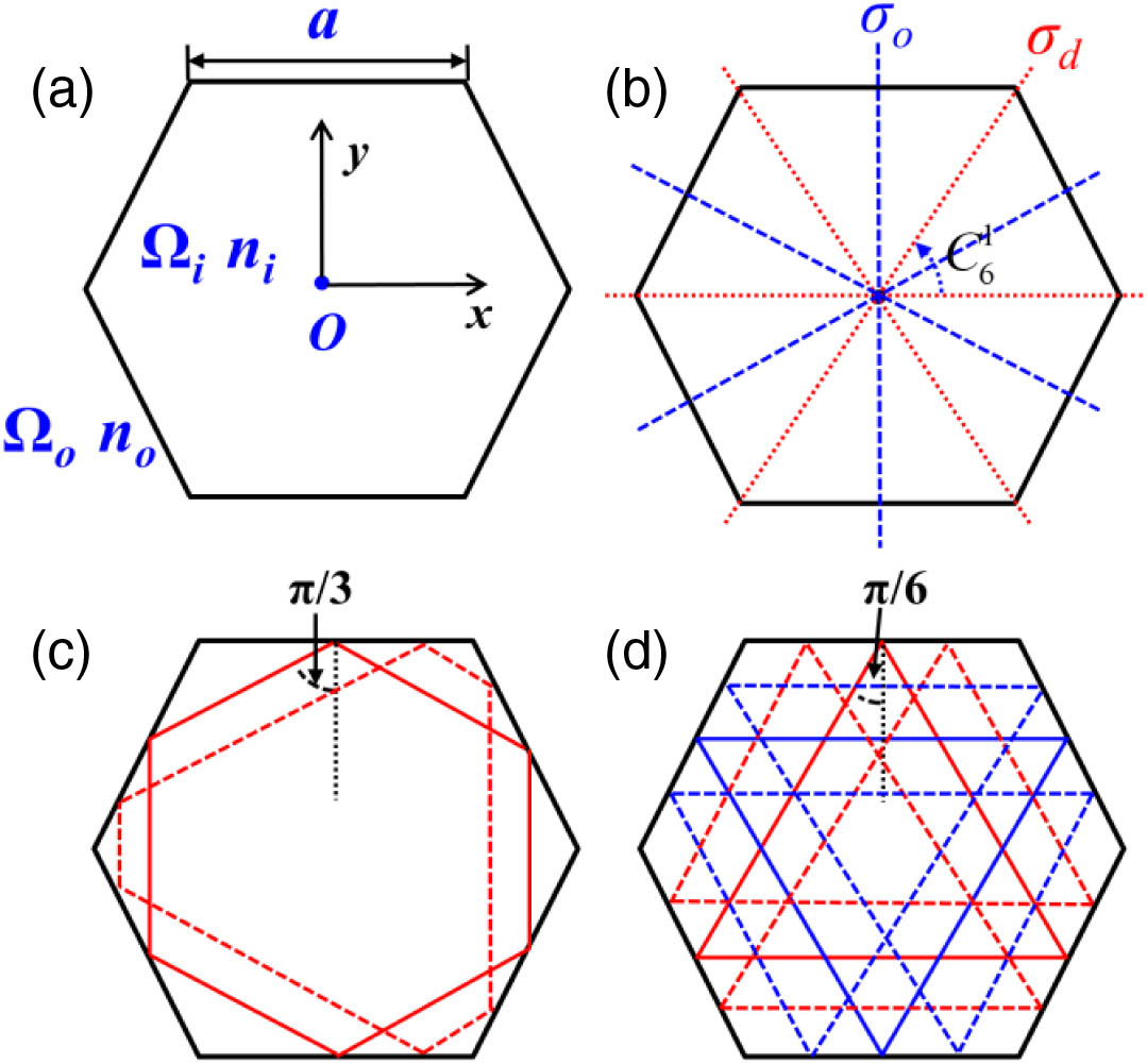
Fig. 1. (a) Schematic diagram and (b) symmetry operators of a 2D hexagonal microcavity. (c) The hexagonal periodic orbits and (d) the triangular periodic orbits in the hexagonal microcavity. The solid lines and dashed lines indicate, respectively, the ray trajectories connecting the midpoints of the sides and the other ray trajectories in the same orbit family with the same incident angles.
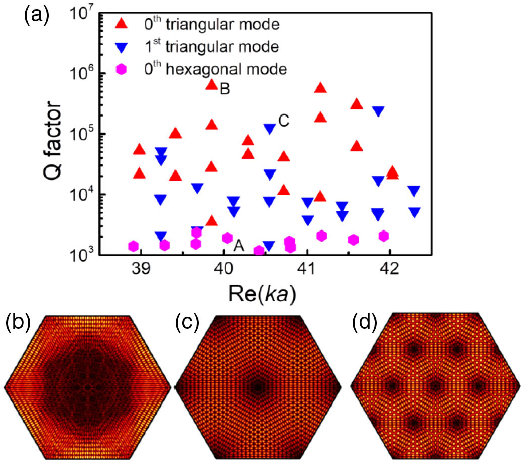
Fig. 2. (a) Simulated TE modes in the hexagonal microcavity with refractive indices of 3.2/1. (b)–(d) The magnetic-field amplitude distributions of the modes marked by A, B, and C.
Fig. 3. (a) Mode Q Q n i / n o
Fig. 4. Mode Q
Fig. 5. Mode Q n i / n o
Fig. 6. Cross-section and top-down SEM images of ZnO nanodisks with diameters of (a) 842 nm, (c) 612 nm, and (e) 491 nm. (b), (d), and (f) Corresponding lasing spectra collected at increasing pump powers. Inset: PL intensity versus pump power. (g) Room temperature lasing threshold versus disk diameter. Reproduced from Ref. [80].
Fig. 7. (a) Emission spectra of a ZnO microrod with a diagonal of 6.67 μm when excited with a Nd:YAG laser at different excitation power densities. Inset: far-field emission image of the lasing ZnO microrod taken with a digital camera. (b) Output lasing intensity versus excitation power density. Reproduced from Ref. [84].
Fig. 8. PL mapping along the ZnO tapered arm for (a) TE and (b) TM polarized modes. Reproduced from Ref. [119].
Fig. 9. SEM images of (a) the bird’s-eye view and (b) the top view of a GaN hexagonal microdisk. (c) Bird’s-eye-view SEM image of the GaN hexagonal microdisk cut with an FIB. (d) Schematic diagram of hexagonal and triangular periodic orbits (called WGM and quasi-WGM here). Reproduced from Ref. [87].
Fig. 10. (a) Schematic diagram of ray path in on-chip nanopillars. (b) FDTD-simulated field profile of a WGM with an angular mode number of 6 in the hexagonal plane. (c) First-order and (d) higher-order transverse modes in the vertical direction. (e) SEM image of a subwavelength device. [(f)–(h)] SEM images and experimental emission patterns of nanopillars. Reproduced from [128].
Fig. 11. (a) Applied voltage and fiber-coupled output power versus continuous-wave injection current, and (b) lasing spectra at different injection currents for a hexagonal microcavity laser with a side length of 10 μm and a 1.5-μm-wide output waveguide. The inset in (a) shows a microscopic image of the hexagonal microcavity laser.
Fig. 12. (a) SEM image of a deformed hexagonal microlaser after inductively coupled plasma etching. (b) Microscopic image of a deformed hexagonal microcavity laser. (c) Applied voltage and fiber-coupled output power versus continuous-wave injection current. (d) Lasing spectra at injection currents of 2.5, 14, and 23 mA. (e) Small-signal responses for the circular-side hexagonal resonator at bias currents of 6, 8, 14, and 21 mA. Reproduced from Ref. [91].
|
Table 1. Character Table of Point Group C 6 v

Set citation alerts for the article
Please enter your email address
© Copyright 2018-2021 | Chinese Laser Press. All Rights Reserved 沪ICP备15018463号-20