
Feng Liang, Degang Zhao, Zongshun Liu, Ping Chen, Jing Yang, Lihong Duan, Yongsheng Shi, Hai Wang. GaN-based blue laser diode with 6.0 W of output power under continuous-wave operation at room temperature[J]. Journal of Semiconductors, 2021, 42(11): 112801
- Journal of Semiconductors
- Vol. 42, Issue 11, 112801 (2021)
Abstract
1. Introduction
III-nitride material and devices have attracted great attention in the past years. GaN-based laser diodes (LDs), including in ultraviolet LDs, violet LDs, blue LDs and green LDs, have wide applications in biomedicine, wireless optical communication, solid-state lighting, laser projector, industrial manufacturing and quantum technology[
2. Experiments
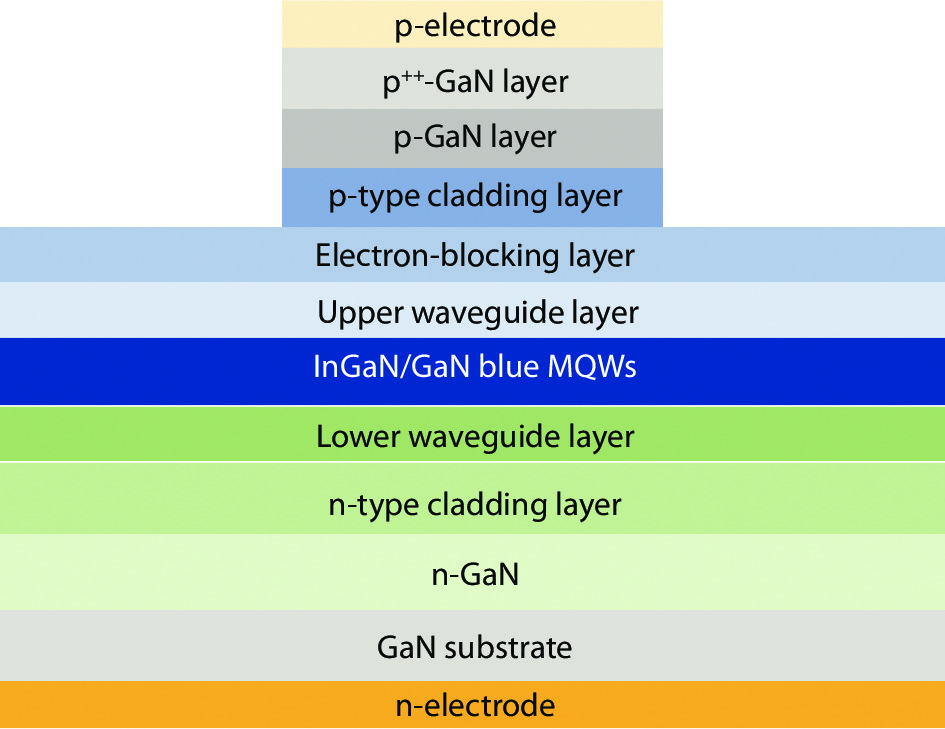
GaN-based blue LD structures are grown on the c-plane GaN substrate by metal organic chemical vapor deposition (MOCVD), and the schematic diagram of the GaN-based blue LDs is shown in Fig. 1. During growth, ammonia (NH3), trimethylgallium (TMGa) or triethylgallium (TEGa), trimethylindium (TMIn) and trimethylaluminum (TMAl) are used as the N, Ga, In and Al precursors, respectively, and the p-type and n-type dopants are di-cyclopentadienyl magnesium (Cp2Mg) and silane (SiH4), respectively. The epitaxial LD structure includes the n-GaN layer, n-type cladding layer, n-type waveguide layer, InGaN/GaN multi-quantum wells (MQW), p-type electron-blocking layer, p-type waveguide layer, p-type cladding layer, p-GaN layer, and the heavily Mg-doped GaN layer (p++-GaN). The ridge waveguide structure is made after epitaxial growth. A 30-μm-wide ridge stripe is fabricated first through photolithography and an etching along the <1-100> direction, and then a 1200- μm-long cavity is formed by cleaving along the {1-100} plane after grounding and polishing the GaN substrate. The front and rear cleaved cavity facets are coated, whose reflectivity is 10% and 90%, respectively. Ti/Pt/Au and Pd/Pt/Au are used for n-type and p-type electrode contacts, respectively. Moreover, photoluminescence imaging in a micro-scale photoluminescence (micro-PL) measurement is performed by using a confocal optical system with a 405 nm-laser excitation (Nikon A1). The output power and power–current–voltage (P–I–V) curves of the GaN-based LDs are measured by a Si-based photodetector and Keithley source meter.
![]()
Figure 1.(Color online) The schematic structure of the GaN-based blue LD chip. The ridge waveguide structure is 30 × 1200
3. Results and discussions
It is well known that the homogeneous emission of MQWs is benefited to improve the optical gain, thus it is one of the key factors to reach a low threshold current and a high output power of GaN-based laser diodes[
![]()
Figure 2.(Color online) Photoluminescence image in micro-scale of a GaN-based blue LD grown on GaN substrate.
The LD chip is fabricated in a size of 1200 μm long and about 100 μm thick, and it is packaged in a C-mount and bonded on a Cu heat sink by indium solder. Fig. 3(a) shows the P–I–V curves of this C-mount packaged GaN-based blue LD, which works under continuous-wave operation at room temperature. It is observed that the optical power increases sharply after lasing starts when the injection current increases to the threshold current about 400 mA. The corresponding threshold current density and threshold voltage is 1.1 kA/cm2 and 4.2 V, respectively. In addition, the peak optical power is larger than 6.0 W under an injection current of 5.0 A, and the corresponding voltage is around 5.7 V. Fig. 3(b) shows the optical spectrum of stimulated emission of the GaN-based blue LD under continuous-wave operation. It can be seen that the peak wavelength is around 442 nm, and its full width at half maximum (FWHM) is about 0.8 nm which is obtained by Gaussian fitting. Such a high optical power is a result of joint effort on improving LD structure design, material epitaxial growth and technological processing of device fabrication.
![]()
Figure 3.(Color online) (a)
It is noted that the threshold voltage and the high output operation voltage is as low as 4.2 and 5.7 V, respectively. Such low voltage values are mainly attributed to our research works on improving p-type material quality and p-GaN Ohmic contact to reduce the series resistance and contact resistance of GaN-based LDs. On one side, a low resistivity of the p-AlGaN layer has been achieved by suppressing the compensation effect of C-related residual donors and coordinately controlling the concentrations of Mg-dopant and hydrogen impurity[
4. Conclusion
In summary, the continuous-wave GaN-based blue LD with 6.0 W optical power operated at room temperature is demonstrated. The stimulated emission wavelength of LD is about 442 nm, and the threshold current density is as low as 1.1 kA/cm2. The blue LD is grown on a c-plane GaN substrate by MOCVD, and fabricated with a 30 × 1200 μm2 ridge waveguide structure.
Acknowledgments
This work was supported by the National Key R&D Program of China (Grant Nos. 2018YFB0406903, 2017YFB0405001, 2016YFB0400803 and 2016YFB0401801), the Science Challenge Project (Grant No. TZ2016003), the National Natural Science Foundation of China (Grant Nos. 62034008, 62074142, 62074140, 61974162, 61904172, and 61874175), the Youth Innovation Promotion Association of Chinese Academy of Sciences (Grant No. 2019115), Beijing Nova Program (Grant No. 202093), Beijing Municipal Science and Technology Project (Grant No. Z161100002116037), Jiangsu Institute of Advanced Semiconductors (IASEMI 2020-CRP-02), and Young Elite Scientists Sponsorship Program by CAST.
References
[1] S Nakamura, M Senoh, S I Nagahama et al. InGaN-based multi-quantum-well-structure laser diodes. Jpn J Appl Phys, 35, L74(1996).
[2] I Akasaki, S Sota, H Sakai et al. Shortest wavelength semiconductor laser diode. Electron Lett, 32, 1105(1996).
[3] Z Zhang, M Kushimoto, T Sakai et al. A 271.8 nm deep-ultraviolet laser diode for room temperature operation. Appl Phys Express, 12, 124003(2019).
[4] D G Zhao, J Yang, Z S Liu et al. Fabrication of room temperature continuous-wave operation GaN-based ultraviolet laser diodes. J Semicond, 38, 051001(2017).
[5] F Liang, D G Zhao, D S Jiang et al. Performance deterioration of GaN-based laser diode by V-pits in the upper waveguide layer. Nanophotonics, 9, 667(2020).
[6] F Liang, J Yang, D G Zhao et al. Room-temperature continuous-wave operation of GaN-based blue-violet laser diodes with a lifetime longer than 1000 h. J Semicond, 40, 022801(2019).
[7] U T Schwarz, E Sturm, V Kümmler et al. Gain spectra and current-induced phase-shift in blue laser diodes. Frontiers in Optics, WMM3(2003).
[8] M Kuramoto, Y Hisanaga, A Kimura et al. An alloy semiconductor system with a tailorable band-tail and its application to high-performance laser operation: II. Experimental study on InGaN MQW laser for optimization of differential gain characteristics tuned by In compositional fluctuation. Semicond Sci Technol, 16, 770(2001).
[9] K Kojima, M Funato, Y Kawakami et al. Gain suppression phenomena observed in In
[10] F Liang, J Yang, D G Zhao et al. Influence of hydrogen impurity on the resistivity of low temperature grown p-Al
[11] X W Wang, F Liang, D G Zhao et al. Improving the homogeneity and quality of InGaN/GaN quantum well exhibiting high In content under low TMIn flow and high pressure growth. Appl Surf Sci, 548, 149272(2021).
[12] X Wang, F Liang, D Zhao et al. Investigations on the optical properties of InGaN/GaN multiple quantum wells with varying GaN cap layer thickness. Nanoscale Res Lett, 15, 191(2020).
[13] L Y Peng, D G Zhao, J J Zhu et al. Achieving homogeneity of InGaN/GaN quantum well by well/barrier interface treatment. Appl Surf Sci, 505, 144283(2020).
[14] J Yang, D G Zhao, D S Jiang et al. Investigation on the compensation effect of residual carbon impurities in low temperature grown Mg doped GaN films. J Appl Phys, 115, 163704(2014).
[15] F Liang, J Yang, D G Zhao et al. Resistivity reduction of low temperature grown p-Al0.09Ga0.91N by suppressing the incorporation of carbon impurity. AIP Adv, 8, 085005(2018).
[16] Y Zhang, F Liang, D Zhao et al. Hydrogen can passivate carbon impurities in Mg-doped GaN. Nanoscale Res Lett, 15, 38(2020).
[17] F Liang, D Zhao, D Jiang et al. Influence of residual carbon impurities in a heavily Mg-doped GaN contact layer on an Ohmic contact. Appl Opt, 56, 4197(2017).
[18] F Liang, D G Zhao, D S Jiang et al. Improvement of Ohmic contact to p-GaN by controlling the residual carbon concentration in p++-GaN layer. J Cryst Growth, 467, 1(2017).

Set citation alerts for the article
Please enter your email address
© Copyright 2018-2021 | Chinese Laser Press. All Rights Reserved 沪ICP备15018463号-20