• Laser & Optoelectronics Progress
  • Vol. 60, Issue 18, 1811017 (2023)
Daoyuan Wang1, Chengzhe Gao1, Wanxia Huang1, Kun Meng2, and Qiwu Shi1、*
Author Affiliations
  • 1College of Materials Science and Engineering, Sichuan University, Chengdu 610065, Sichuan , China
  • 2Qingdao QUNDA Terahertz Technology Co., Ltd., Qingdao 266104, Shandong , China
  • show less
    DOI: 10.3788/LOP231068 Cite this Article Set citation alerts
    Daoyuan Wang, Chengzhe Gao, Wanxia Huang, Kun Meng, Qiwu Shi. Terahertz Wave Reflection Regulation Based on Controllable Impedance of Silicon-Based MXene Layers[J]. Laser & Optoelectronics Progress, 2023, 60(18): 1811017 Copy Citation Text show less
    Schematic of the impedance matching model. (a) THz transmission through pure Si substrate; (b) THz transmission through Si/MXene film
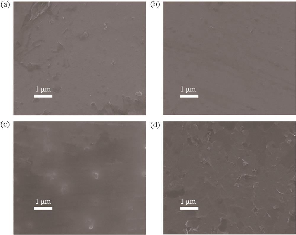
    Fig. 1. Schematic of the impedance matching model. (a) THz transmission through pure Si substrate; (b) THz transmission through Si/MXene film
    SEM morphology of MXene film with different stacking layers. (a) 1 layer; (b) 2 layers; (c) 4 layers; (d) 8 layers
    Fig. 2. SEM morphology of MXene film with different stacking layers. (a) 1 layer; (b) 2 layers; (c) 4 layers; (d) 8 layers
    Schematic of the relationship between THz wave reflection signal and MXene film thickness under different incident angles. (a) 30°; (b) 40°; (c) 50°; (d) 55°
    Fig. 3. Schematic of the relationship between THz wave reflection signal and MXene film thickness under different incident angles. (a) 30°; (b) 40°; (c) 50°; (d) 55°
    Schematic of the normalized THz reflected signals as a function of MXene with different stacking film layers under different angles. (a) 30°; (b) 40°; (c) 50°; (d) 55°
    Fig. 4. Schematic of the normalized THz reflected signals as a function of MXene with different stacking film layers under different angles. (a) 30°; (b) 40°; (c) 50°; (d) 55°
    THz reflection imaging result at the Air/ Si interface changing with MXene with different stacking film layers at Si substrate. (a) 1 layer; (b) 3 layers; (c) 6 layers; (d) 8 layers
    Fig. 5. THz reflection imaging result at the Air/ Si interface changing with MXene with different stacking film layers at Si substrate. (a) 1 layer; (b) 3 layers; (c) 6 layers; (d) 8 layers
    THz reflection imaging result at the Si/MXene/Air interface changing with MXene with different stacking film layers. (a) 1 layer; (b) 3 layers; (c) 4 layers; (d) 5 layers; (e) 6 layers; (f) 8 layers
    Fig. 6. THz reflection imaging result at the Si/MXene/Air interface changing with MXene with different stacking film layers. (a) 1 layer; (b) 3 layers; (c) 4 layers; (d) 5 layers; (e) 6 layers; (f) 8 layers
    THz transmission intensity of the samples changing with MXene with different stacking film layers. (a) Time-domain spectra of THz-wave transmission; (b) normalized THz transmission
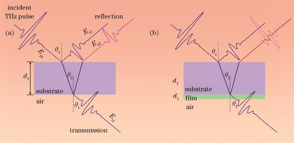
    Fig. 7. THz transmission intensity of the samples changing with MXene with different stacking film layers. (a) Time-domain spectra of THz-wave transmission; (b) normalized THz transmission
    Daoyuan Wang, Chengzhe Gao, Wanxia Huang, Kun Meng, Qiwu Shi. Terahertz Wave Reflection Regulation Based on Controllable Impedance of Silicon-Based MXene Layers[J]. Laser & Optoelectronics Progress, 2023, 60(18): 1811017
    Download Citation