Preparing organic light-emitting diode (OLED) displays by inkjet printing technology is a research direction for next-generation display technologies. This technology is a material-saving deposition technology characterized by simple process, low cost, low power consumption, and capability for mass production, and it has thus been widely used in the electronics industry. The inkjet printing process imposes an extremely strict requirement on the accuracy of the process parameters, and printing defects are prone to occur when the parameters are outside the error ranges. In the preparation process, the printed OLED pixel image consists of repetitive and equally spaced horizontal and vertical lines, and this background texture varies with illumination conditions. The variation in texture, the low contrast of the defective pixels, and the changing size of the defective area pose a great challenge to the detection of printing defects. The possible printing defects are divided into two main categories: film-forming integrity defects in printed OLED pixels and film thickness uniformity defects in printed OLED pixels. Among them, film-forming integrity defects include the presence of satellite points, failure to cover the whole bank, overflow of overlarge ink droplets from the bank, and a mix of multiple types of defects. Automatic optical inspection (AOI) technology is widely used for the detection of OLED defects. Although most of the existing methods achieve favorable results in detecting the defects on the OLED panel surface, they tend to ignore the detailed features of defects in printed OLED pixels when they are applied to detect such defects. They are insufficient in the cases of limited printed pixel images and tiny pixel defects and consequently fail to deliver favorable results in pixel defect detection when the quality of printed OLED pixel images is reduced. To effectively improve the accuracy of the detection of OLED pixel defects and achieve the intelligent detection of inkjet-printed OLED pixel defects, this paper proposes an extended feature pyramid network (FPN) and applies it to the task of detecting OLED pixel defects.
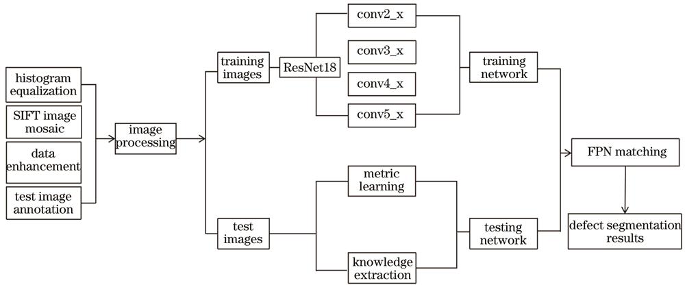
The features are enhanced by fusing the feature pyramids at different levels. A dedicated feature extraction module for small targets is added to enhance the sensitivity of the detection of OLED pixel defects. Then, an additional high-resolution pyramid layer is used to extract credible regional details, and the channel capacity is reduced by fusing the two pyramid layers at bottom to fully utilize the information from the underlying feature map. Finally, transfer learning is applied to limited samples to address the problem of low goodness of fit caused by insufficient sample data.
This paper proposes a detection method for OLED pixel defects based on an extended FPN. According to the features of inkjet-printed OLED pixel defects, the paper extends the original FPN, effectively obtains regional details at different levels of the hierarchy, and integrates semantic information from higher levels in a pyramidal manner to enrich the underlying features and enhance the contrast of details. More accurate detection of OLED pixel defects is thereby achieved. In addition, combined with ResNet18, the method proposed in this paper attains a robust generalization ability for a limited amount of OLED pixel image data. The results show that compared with other methods, the proposed method demonstrates superior performance, with a defect detection rate of 99.8% and a defect segmentation accuracy of 88.8% on the inkjet-printed OLED pixel dataset. Therefore, the proposed method can achieve favorable detection results on such small sample datasets and largely meets the industrial demand of OLED mass production in large sizes.