
Jin YANG, Jin-Cheng KONG, Jian-Yun YU, Yan-Hui LI, Chun-Zhang YANG, Gang QIN, Dong-Sheng LI, Wen LEI, Jun ZHAO, Rong-Bin JI. The ‘swallow-tailed defect’ in MBE HgCdTe film [J]. Journal of Infrared and Millimeter Waves, 2020, 39(6): 690
- Journal of Infrared and Millimeter Waves
- Vol. 39, Issue 6, 690 (2020)
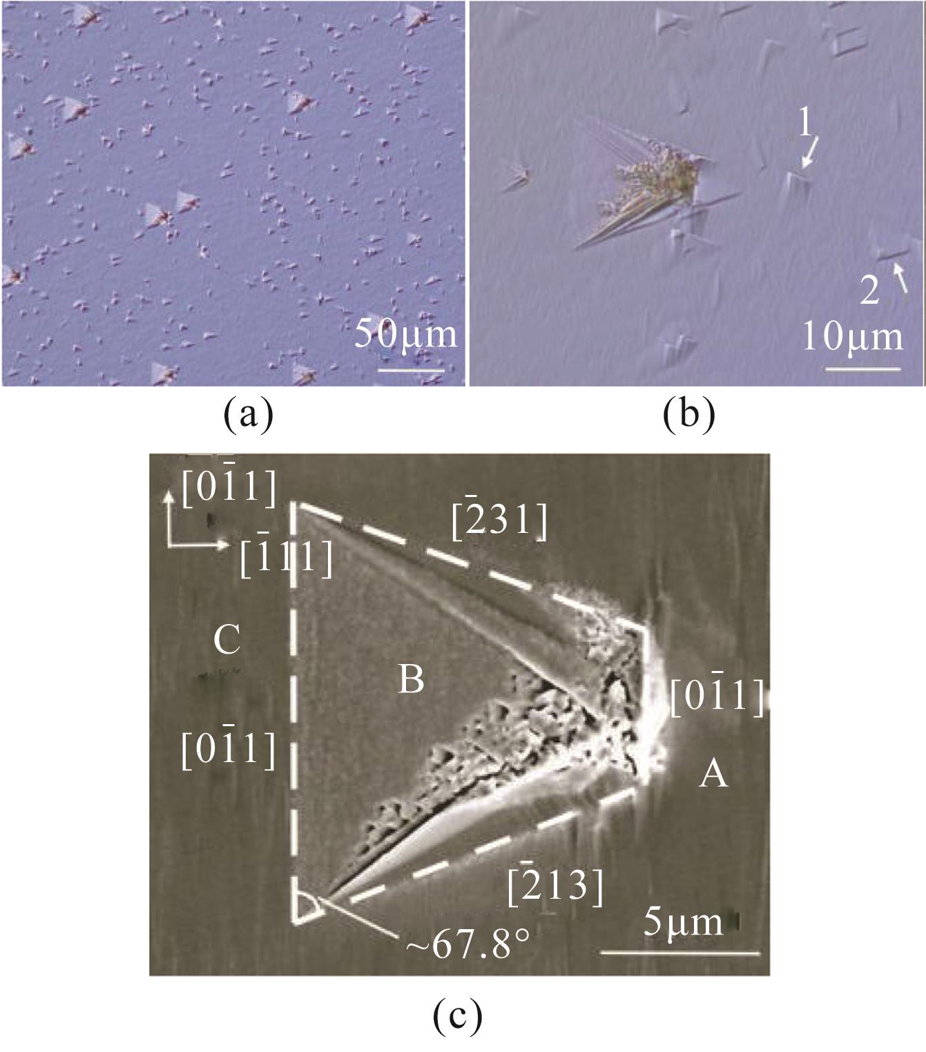
Fig. 1. Surface topography of the swallow-tailed defect (a) optical microscope images with 200 magnification, (b) optical microscope images with 1000 magnification, (c) SEM image ,Note(s): The arrays in (b) show different direction of raised side in triangle defect. The four dash lines in (c) are outlines of the defect. Capital A, B, C in (c) represent three EDS test areas.
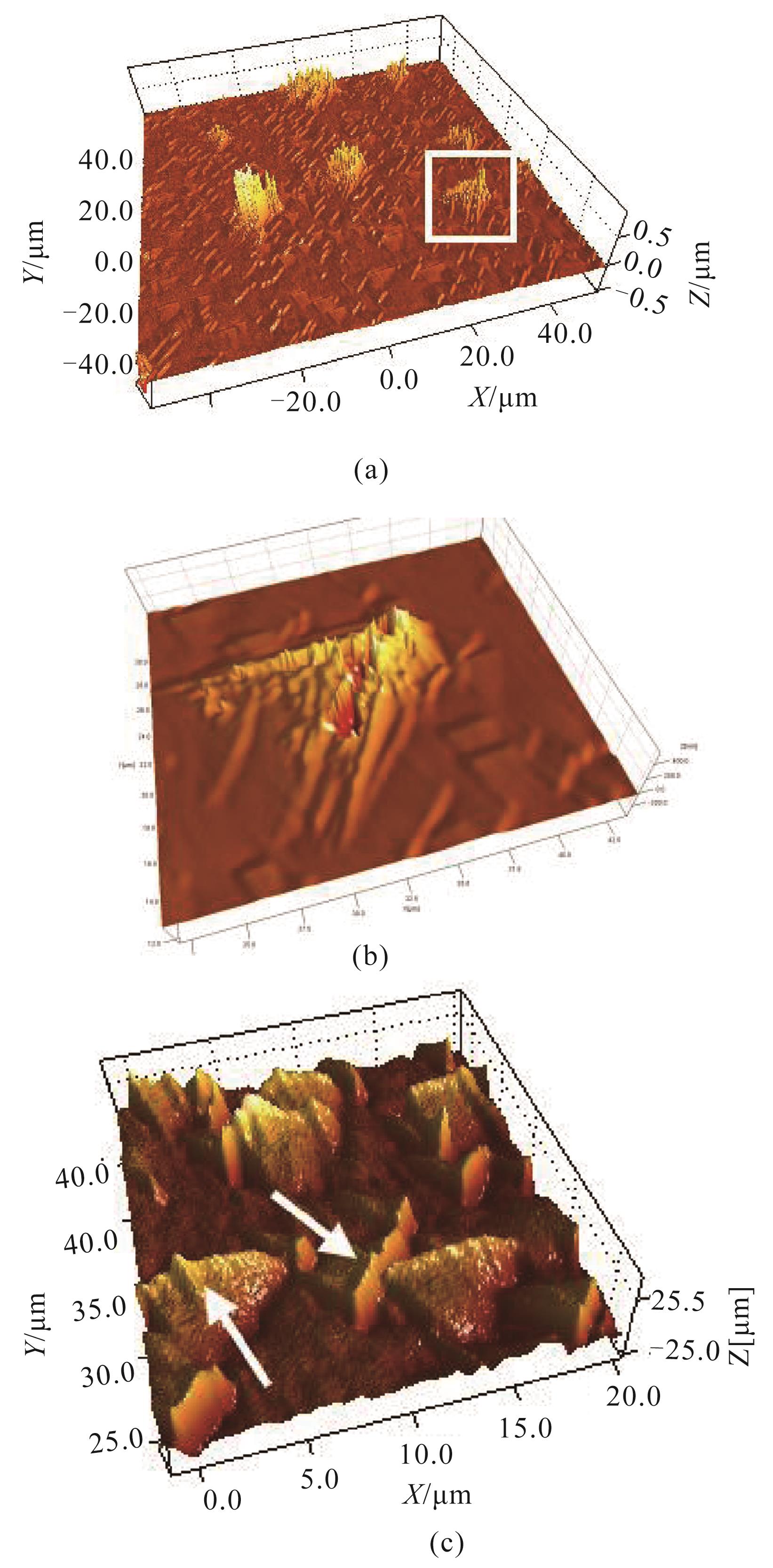
Fig. 2. White light interferometry images of HgCdTe surface (a) 100 μm×100 μm area,(b) defect marked in figure (a),(c) triangular defects.
Fig. 3. Cross-sectional SEM images at different positions, the cross-sectional plane is ( 1 1 ¯ 1 ¯ ) ![]()
![]()
Fig. 4. Structure of swallow-tailed defect in epi-layer (a) Schematic graph, (b) defect structure from Diamond software.
Fig. 5. HRXRD omega-2theta scan pattern, (a) HgCdTe with swallow-tailed defect, (b) single crystal HgCdTe, (c) CdTe buffer of HgCdTe with swallow-tailed defect, (d) CdTe buffer of single crystal HgCdTe
Fig. 6. Schematic of different atomic sequence along [111] direction of (211) and (552) grain.
Fig. 7. Bright field microscopy images of CdTe after Everson etching (a)the typical triangle etch pits observed on type-I CdTe, (b)surface turned to black and no etch pit found in Type-II CdTe
Fig. 8. Bright field microscopy images of Te-terminated CdTe and Cd-terminated CdTe (a) Te-terminated CdTe,(b)Cd-terminated CdTe
Fig. 9. HRXRD ω -2θ scan pattern (a) 2 μm HgCdTe on CdTe/Ge, (b) 2 μm CdTe on Ge
|
Table 1. “燕尾”状缺陷内及附近碲镉汞组分值

Set citation alerts for the article
Please enter your email address
© Copyright 2018-2021 | Chinese Laser Press. All Rights Reserved 沪ICP备15018463号-20