• Chinese Optics Letters
  • Vol. 18, Issue 11, 112501 (2020)
Chunhong Zeng1、2, Wenkui Lin2, Tao He2、3, Yukun Zhao2, Yuhua Sun2, Qi Cui2, Xuan Zhang2, Shulong Lu2, Xuemin Zhang2, Yameng Xu1, Mei Kong1、*, and Baoshun Zhang2、**
Author Affiliations
  • 1School of Science, Changchun University of Science and Technology, Changchun 130022, China
  • 2Suzhou Institute of Nano-Tech and Nano-Bionics, Chinese Academy of Sciences, Suzhou 215123, China
  • 3School of Materials Science and Engineering, Nanjing University of Science and Technology, Nanjing 210094, China
  • show less
    DOI: 10.3788/COL202018.112501 Cite this Article Set citation alerts
    Chunhong Zeng, Wenkui Lin, Tao He, Yukun Zhao, Yuhua Sun, Qi Cui, Xuan Zhang, Shulong Lu, Xuemin Zhang, Yameng Xu, Mei Kong, Baoshun Zhang. Ultraviolet-infrared dual-color photodetector based on vertical GaN nanowire array and graphene[J]. Chinese Optics Letters, 2020, 18(11): 112501 Copy Citation Text show less
    (a) SEM morphology of the vertical GaN nanowire array; (b) HRTEM image of a single GaN nanowire; (c) XRD pattern of the vertical GaN nanowire array; (d) Raman spectrum of the monolayer graphene film.
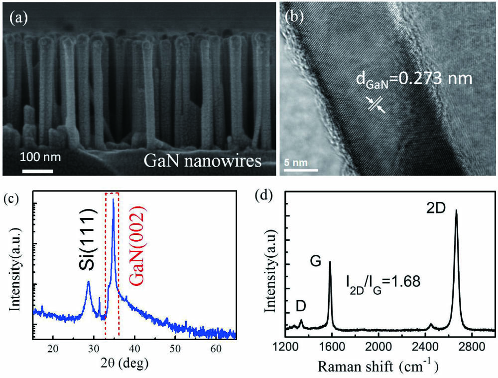
    Fig. 1. (a) SEM morphology of the vertical GaN nanowire array; (b) HRTEM image of a single GaN nanowire; (c) XRD pattern of the vertical GaN nanowire array; (d) Raman spectrum of the monolayer graphene film.
    (a) Schematic diagram of the UV-IR dual-color detector based on GaN/graphene heterojunction; (b) optical microscopy image of the top of the fabricated device.
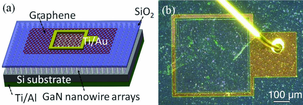
    Fig. 2. (a) Schematic diagram of the UV-IR dual-color detector based on GaN/graphene heterojunction; (b) optical microscopy image of the top of the fabricated device.
    Energy band and carrier transition diagrams of the graphene/GaN nanowire heterojunction under illumination.
    Fig. 3. Energy band and carrier transition diagrams of the graphene/GaN nanowire heterojunction under illumination.
    (a) I–V characteristic of the device measured at room temperature in the dark. The inset shows the H versus I used to estimate φB at the graphene/GaN heterojunction; (b) spectral response of the detector at a bias of −5 V; (c) peak responsivities of the detector under different bias voltages at different wavelengths; (d) dark current and output photocurrent versus bias at 360 nm and 1540 nm.
    Fig. 4. (a) I–V characteristic of the device measured at room temperature in the dark. The inset shows the H versus I used to estimate φB at the graphene/GaN heterojunction; (b) spectral response of the detector at a bias of 5V; (c) peak responsivities of the detector under different bias voltages at different wavelengths; (d) dark current and output photocurrent versus bias at 360 nm and 1540 nm.
    Schematic of the transient spectral response test system.
    Fig. 5. Schematic of the transient spectral response test system.
    (a) and (b) Multi-periodic and monocycle transient response of the device to 365 nm LED irradiation; (c) and (d) multi-periodic and monocycle transient response of the device to 1500 nm LED irradiation.
    Fig. 6. (a) and (b) Multi-periodic and monocycle transient response of the device to 365 nm LED irradiation; (c) and (d) multi-periodic and monocycle transient response of the device to 1500 nm LED irradiation.
    Wave bandPeak wavelength (nm)R(A/W)D* (cm·Hz1/2·W1)EQE (%)
    UV3606.931.23×10122382
    IR15400.111.88×10108
    Table 1. Parameters of the UV-IR Dual-Color Photodetector at 5V Bias
    Chunhong Zeng, Wenkui Lin, Tao He, Yukun Zhao, Yuhua Sun, Qi Cui, Xuan Zhang, Shulong Lu, Xuemin Zhang, Yameng Xu, Mei Kong, Baoshun Zhang. Ultraviolet-infrared dual-color photodetector based on vertical GaN nanowire array and graphene[J]. Chinese Optics Letters, 2020, 18(11): 112501
    Download Citation