Abstract
A monolithic integrated ultraviolet-infrared (UV-IR) dual-color photodetector based on graphene/GaN heterojunction was fabricated by vertically integrating a GaN nanowire array on a silicon substrate with monolayer graphene. The device detects UV and IR lights by different mechanisms. The UV detection is accomplished by the forbidden band absorption of GaN, and the IR detection is realized by the free electron absorption of graphene. At peak wavelengths of 360 nm and 1540 nm, the detector has responsivities up to 6.93 A/W and 0.11 A/W, detection efficiencies of 1.23 × 1012 cm·Hz1/2 ·W-1 and 1.88 × 1010 cm·Hz1/2 ·W-1, respectively, and a short response time of less than 3 ms.The ultraviolet-infrared (UV-IR) dual-color photodetector is one of the research hotspots of photodetectors, which has important applications in many fields, such as early warning, fire detection, and elemental analysis. Since a UV-IR dual-color photodetector responds to the two different bands simultaneously, it can do better in recognizing targets and avoiding false alarm than a single-band one[1]. In recent years, with the development of the epitaxial technology of wide bandgap semiconductors and the energy band theory, the single integrated UV-IR dual-color detector has become a new research direction. For example, there are some UV/IR dichroic detectors based on the AlGaN/GaN quantum structure[2,3] or ZnO/PbS structure[4,5]. Hofstetter et al. monolithically integrated a UV and an IR detectors on a sapphire substrate, in which the superlattice with GaN quantum wells (QWs) and AlN barriers accomplished the IR perception, and the AlGaN thin film serves as the active area for the ultraviolet detector[6]. Rong et al. proposed a multi-period step-QW structure, which solved the problem of polarization electric field in AlGaN/GaN QWs, reduced the dark current, and improved the response ability of the detector[7]. However, the difficulties in high-quality crystal growth and the unsatisfactory IR characteristics limit the application of the UV-IR dual-color photodetector.
Meanwhile, the development of two-dimensional (2D) materials, especially graphene, brings some new opportunities to photoelectric detection[8]. Graphene has an ultra-wide responding spectrum and can be modulated extremely quickly, which makes it a very attractive photoelectric detection material[9]. However, due to its low overall optical absorption (about 2.3%) and short carrier lifetime [on the order of picoseconds (ps)][10], the responsivity of pure graphene photodetectors is not high, usually only tens of micro-amperes/watt (mA/W) or even less. To enhance the photoelectric response characteristics of semiconductors and play to the strengths of graphene, detectors with graphene bound to various semiconductors, such as Si, Ga2O3, and GaN, have been proposed[11–13]. The results prove that graphene-semiconductor heterojunctions have been a great help to improve the detection performance of the devices.
Compared to a GaN film, vertical GaN nanowire arrays have higher optical absorption, wider response spectrum, better optical coupling, and band-changing ability due to its quantum size, super-high surface-volume ratio, and tunneling effect[14–16]. Nevertheless, most of the reported GaN nanowires are realized by synthesis or secondary growth. For example, nanowires are transformed into GaN nanowires by heating for a long time in a quartz-tube furnace. This increases the complexity and the cost of devices[17,18].
Sign up for Chinese Optics Letters TOC. Get the latest issue of Chinese Optics Letters delivered right to you!Sign up now
In this Letter, for the first time, to the best of our knowledge, a UV-IR dual-color photodetector based on the graphene and vertical GaN nanowire array is proposed and achieved. It makes full use of the excellent properties of the two materials. Photoelectric detection is implemented by the heterojunction composed of them. Absorption enhancement is achieved by multiple reflections in the GaN nanowire array. The higher transparency of the graphene electrode than a metal one benefits the responsivity as well[19,20]. Compared with currently available UV-IR dual-color detectors, this detector has the advantages of simple preparation, high responsivity, and fast response speed.
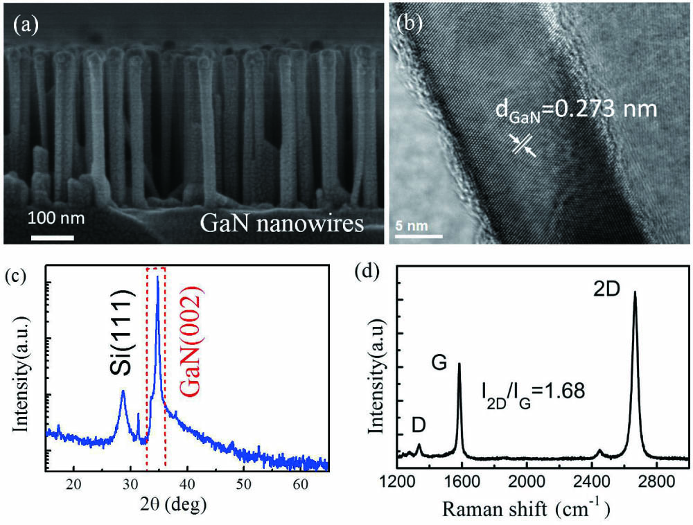
The vertical GaN nanowire arrays were grown along the [002] direction of an -type Si substrate with a resistivity within by molecular beam epitaxy (MBE). The morphology of the GaN nanowire arrays was characterized by a scanning electron microscope (SEM), as shown in Fig. 1(a). Their heights are very uniform (about 300 nm), and the diameters vary from 20 to 50 nm. In order to directly observe the crystallization quality of the GaN nanowire, high-resolution transmission electron microscopy (HRTEM) was applied. The HRTEM image of a single nanowire is shown in Fig. 1(b), which illustrates a good crystallization quality without obvious defects. The atomic spacing is 0.273 nm, which accords with that of the (002) crystal plane of GaN. The microstructure and the composition of the samples were measured by powder X-ray diffraction (XRD). As shown in Fig. 1(c), the GaN (002) peak appears at 34.56°. This result is consistent with that given by HRTEM.

Figure 1.(a) SEM morphology of the vertical GaN nanowire array; (b) HRTEM image of a single GaN nanowire; (c) XRD pattern of the vertical GaN nanowire array; (d) Raman spectrum of the monolayer graphene film.
The monolayer graphene was grown on a Cu film by chemical vapor deposition (CVD). It was transferred to the surface of GaN nanowires array by wet etching. As shown in the Raman spectrum of the transferred graphene [Fig. 1(d)], the 2D peak intensity is significantly higher than that of the G peak, indicating that the transferred graphene is a single-layer structure.
Our UV-IR dual-color photodetector adopts a vertically integrated structure, as shown in Fig. 2(a). The area of the photosensitive surface of the detector is . The back electrode and the ohmic contact were formed by electron beam evaporation of Ti/Al (20/100 nm) and annealing at 400°C for 30 min. The 75-nm-thick insulator layer was prepared by inductively coupled plasma CVD. The photosensitive region was defined by selectively exposing and etching in the photosensitive region. The graphene was transferred to the top of the GaN nanowires by wet transfer to form a transparent electrode. Finally, the front electrode (Ti/Au of 20/150 nm) was evaporated on the graphene. Figure 2(b) is an optical microscope image of the fabricated device.
Figure 2.(a) Schematic diagram of the UV-IR dual-color detector based on GaN/graphene heterojunction; (b) optical microscopy image of the top of the fabricated device.
Figure 3 demonstrates the energy band and the carrier transition diagrams of the graphene/GaN nanowires heterojunction under illumination. The design idea of this detector is as follows: the unintentionally doped graphene is a weak -type material. Due to the contact of the graphene and the GaN nanowire array, a heterojunction will be formed[21]. At no illumination, the barrier between GaN and graphene decreases as a forward bias is applied, and the current increases exponentially. With a reverse bias, the barrier height increases, the depletion region widens, and the current is limited. Because the bandgap of GaN is less than the energy of a UV photon, when the detector is irradiated by UV light, photogenerated carriers will be generated in the GaN nanowires. Here, the GaN nanowires act as a photosensitive material, and the graphene works as a transparent electrode. The photogenerated carrier pairs will be quickly separated and collected on the electrode by the built-in electric field in the space charge region. That is the photocurrent. In the near-IR band, graphene can absorb about 2.3% of vertical incident light in a wide spectral range[8,22]. When IR light is irradiated on the graphene surface, the transition rate of the photoexcited hot electrons may be greater than the carrier recombination rate. The photogenerated carriers of energy greater than the barrier between graphene and GaN can leap over the barrier and form a photocurrent.
Figure 3.Energy band and carrier transition diagrams of the graphene/GaN nanowire heterojunction under illumination.
Firstly, the basic electrical characteristics of the UV-IR dual-color detector are tested and calculated. The current–voltage (I–V) characteristic is illustrated in Fig. 4(a). The Schottky barrier height can be extracted from the I–V curve[23]. Through the linear fitting of the data in the inset of Fig. 4(a), the barrier height () is estimated as 0.82 eV. This value is comparable to previously reported results for the graphene/GaN heterojunction[24].
Figure 4.(a) I–V characteristic of the device measured at room temperature in the dark. The inset shows the H versus I used to estimate at the graphene/GaN heterojunction; (b) spectral response of the detector at a bias of ; (c) peak responsivities of the detector under different bias voltages at different wavelengths; (d) dark current and output photocurrent versus bias at 360 nm and 1540 nm.
Secondly, in order to assess the optical characteristics of the detector, its spectral response to the UV and IR bands is measured. The detector is tested by a self-built response testing system[25]. Two standard detectors are used to calibrate the intensity of the light source (a xenon lamp) in UV and IR bands, respectively. For example, the power densities of the light source are evaluated as and at 360 nm and 1540 nm, respectively. The phase-locked amplifier is used to measure the photocurrent of the detector, so as to calculate the photoelectric response spectrum of the detector. Figure 4(b) shows the photoelectric response spectra of the detector at a bias. The maximum responsivity is 6.93 A/W at 360 nm. The response wavelength is in agreement with the band gap of GaN of 3.4 eV. Since the response of both graphene and Si is weak below 400 nm[26], as we have aspired above, this is the response of the GaN nanowires. Because Si strongly responds in both visible and near-IR bands with a cutoff wavelength of 1100 nm, the peak in the 500–1100 nm range is mainly contributed by the Si substrate. The response above 1100 nm comes from graphene. The peak wavelength of the 1540 nm in this band coincides with the previously calculated barrier height of 0.82 eV between graphene and GaN, which corresponds to a light wavelength of 1510 nm.
In this Letter, since we focus on the response of the combination of the GaN nanowire array and the graphene, and such a structure can also be grown on other substrates, in the following, only the dual-color response around 360 nm and 1540 nm will be considered. In future work, to remove the influence of Si material on the response spectrum, we will explore replacing the Si substrate by other materials, such as SiC, using a GaN self-supporting substrate, or growing a GaN film on a Si substrate as the lower electrode support material and then growing GaN nanowires on it.
The responsivity at the peak wavelengths of 360 nm and 1540 nm at different reverse bias voltages is measured and shown in Fig. 4(c). It was found that in both bands, the responsivity of the device increases with the increase of the bias voltage. The photocurrents of the detector under the xenon lamp irradiation at 360 nm and 1540 nm were measured, as shown in Fig. 4(d). They are far greater than the dark current at a large bias. These test results fully prove the UV-IR dual-color detection performance of the device.
Another two figures of merit for a detector are detection efficiency () and external quantum efficiency (), which can be calculated by where , , , , , , and are the junction area, responsivity, dark current, Planck constant, speed of light, electronic charge, and wavelength, respectively. represents the sensitivity of the device, and indicates the sufficiency of electron transport as well as carrier collection. The parameters of the UV-IR dual-color detector are summarized in Table 1.
| Wave band | Peak wavelength (nm) | R(A/W) | D* (cm·Hz1/2 · W−1) | EQE (%) |
|---|
| UV | 360 | 6.93 | 1.23×10¹² | 2382 |
| IR | 1540 | 0.11 | 1.88×10¹⁰ | 8 |
Table 1. Parameters of the UV-IR Dual-Color Photodetector at Bias
The responsivity of the detector is much higher than those of the traditional UV detectors (typically 150–300 mA/W)[27] and the monolayer graphene detectors (typically 1–10 mA/W)[28,29]. The reasons are expected to be as follows. (1) As the GaN nanowire array has high surface-volume ratio, the photosensitive area of UV light increases. (2) A microcavity structure is formed by the graphene and GaN nanowires. When light enters the nanowire array, it is reflected multiple times in the nanowire array. This is equivalent to an increase of the absorption area and enhances the light-trapping ability of the detector. (3) Compared with ordinary electrodes, graphene is transparent for UV transmission. (4) The heterojunction formed between the graphene and the GaN nanowire array promotes the separation of the photogenerated carrier pairs and enlarges the photocurrent.
Lastly, the transient response characteristics of our detector are measured by the test system shown in Fig. 5. The detector is illuminated by a 365 nm LED and a 1500 nm one, respectively. The switching frequency of the LED is controlled by a frequency generator. The bias voltage of the detector is , and the photoelectric signal obtained by the detector is detected by an oscilloscope. It can be seen from Figs. 6(a) and 6(b) that for the UV light, the rise time of the device, defined as the time when the current increases from 10% to 90% of the peak value, is 0.36 ms, and the attenuation time, defined as the time when the current drops from 90% to 10% of it, is 1.22 ms. For the IR illumination, from Figs. 6(c) and 6(d), they are 0.76 ms and 2.68 ms, respectively. These data indicate that the response speed of our detector is in the leading level compared to similar GaN nanowire-based detectors reported (typically 20–200 ms)[30]. Besides the contribution of the heterojunction, the rapid response performance of our detector is also attributed to the excellent crystal quality of the GaN nanowires, because the fewer defects there are in the crystal, the fewer carriers will be captured, and the faster the detector will respond.
Figure 5.Schematic of the transient spectral response test system.
Figure 6.(a) and (b) Multi-periodic and monocycle transient response of the device to 365 nm LED irradiation; (c) and (d) multi-periodic and monocycle transient response of the device to 1500 nm LED irradiation.
In summary, a UV-IR dual-color photodetector based on integration of monolayer graphene and a vertical GaN nanowire array was designed, fabricated, and evaluated. The device has two response peaks at 360 nm and 1540 nm, respectively. At these two wavelengths, the responsivities are 6.93 A/W and 0.11 A/W, and the response times of the device are less than 3 ms. The heterojunction structure formed by the graphene and vertical GaN nanowire array improves the performance of devices. Besides that, the high surface-volume ratio of the GaN nanowire array and the microcavity formed by the graphene and nanowires enhance the photon capture ability in the UV and IR bands. At the same time, graphene as a transparent electrode plays an important role in the high-response performance of the device. It should be noted that GaN nanowires can also be used to design ternary alloy-based AlGaN nanowires to extend the spectral response range. The UV response wavelength of the UV-IR dual-color detector can reach the solar-blind UV spectrum range. Therefore, the graphene/vertical GaN nanowire array may be the next candidate for future development of UV-IR dual-color detectors.
References
[1] A. G. U. Perera, G. Ariyawansa, M. B. M. Rinzan, M. Stevens, M. Alevli, N. Dietz, S. G. Matsik, A. Asghar, I. T. Ferguson, H. Luo, A. Bezinger, H. C. Liu. Infrared Phys. Techn., 50, 142(2007).
[2] H. J. Huang, D. W. Yan, G. S. Wang, F. Xie, G. F. Yang, S. Q. Xiao, X. F. Gu. Chin. Opt. Lett., 12, 092301(2014).
[3] G. Ariyawansa, M. B. M. Rinzan, M. Alevli, M. Strassburg, N. Dietz, A. G. U. Perera, S. G. Matsik, A. Asghar, I. T. Ferguson, H. Luo, A. Bezinger, H. C. Liu. Appl. Phys. Lett., 89, 091113(2006).
[4] P. V. V. Jayaweera, P. K. D. D. P. Pitigala, J. F. Shao, K. Tennakone, A. G. U. Perera, P. M. Jayaweera, J. Baltrusaitis. IEEE Trans. Electron. Dev., 57, 2756(2010).
[5] Q. Li, J. Bai, Y. Q. Lv, W. D. Hu, X. S. Chen, W. Lu. J. Infrared Millim. W., 36, 385(2017).
[6] D. Hofstetter, R. Theron, E. Baumann, F. R. Giorgetta, S. Golka, G. Strasser, F. Guillot, E. Monroy. Electron. Lett., 44, 986(2008).
[7] X. Rong, X. Q. Wang, G. Chen, X. T. Zheng, P. Wang, F. J. Xu, Z. X. Qin, N. Tang, Y. H. Chen, L. W. Sang, M. Sumiya, W. K. Ge, B. Shen. Sci. Rep.-UK, 5, 14386(2015).
[8] R. R. Nair, P. Blake, A. N. Grigorenko, K. S. Novoselov, T. J. Booth, T. Stauber, N. M. R. Peres, A. K. Geim. Science, 320, 1308(2008).
[9] J. H. Hu, J. Fu, X. H. Liu, D. P. Ren, J. J. Zhao, Y. Q. Huang. Chin. Opt. Lett., 17, 010501(2019).
[10] T. Winzer, A. Knorr, E. Malic. Nano. Lett., 10, 4839(2010).
[11] B. Y. Liu, C. Y. You, C. Zhao, G. L. Shen, Y. W. Liu, Y. F. Li, H. Yan, Y. Z. Zhang. Chin. Opt. Lett., 17, 020002(2019).
[12] T. He, Y. K. Zhao, X. D. Zhang, W. K. Lin, K. Fu, C. Sun, F. F. Shi, X. Y. Ding, G. H. Yu, K. Zhang, S. L. Lu, X. P. Zhang, B. S. Zhang. Nanophoton., 7, 1557(2018).
[13] F. Lin, S. W. Chen, J. Meng, G. Tse, X. W. Fu, F. J. Xu, B. Shen, Z. M. Liao, D. P. Yu. Appl. Phys. Lett., 105, 073103(2014).
[14] R. Calarco, M. Marso, T. Richter, A. I. Aykanat, R. Meijers, A. V. Hart, T. Stoica, H. Luth. Nano Lett., 5, 981(2005).
[15] F. Gonzalez-Posada, R. Songmuang, M. Den Hertog, E. Monroy. Nano Lett., 12, 172(2012).
[16] Y. L. Zheng, W. L. Wang, Y. Li, J. Y. Lan, Y. Xia, Z. C. Yang, X. B. He, G. Q. Li. ACS Appl. Mater. Inter., 11, 3589(2019).
[17] W. Y. Weng, T. J. Hsueh, S. J. Chang, S. B. Wang, H. T. Hsueh, G. J. Huang. IEEE J. Sel. Top. Quantum. Electron., 17, 996(2011).
[18] J. Li, X. Xi, S. Lin, Z. H. Ma, X. D. Li, L. X. Zhao. ACS Appl. Mater. Inter., 12, 11965(2020).
[19] A. V. Babichev, H. Zhang, P. Lavenus, F. H. Julien, A. Y. Egorov, Y. T. Lin, L. W. Tu, M. Tchernycheva. Appl. Phys. Lett., 103, 201103(2013).
[20] X. Li, T. Sun, K. Zhou, X. Hong, X. Y. Tang, D. C. Wei, W. L. Feng, J. Shen, D. P. Wei. Nanotechnology, 31, 3525(2020).
[21] G. Kalita, M. D. Shaarin, B. Paudel, R. Mahyavanshi, M. Tanemura. Appl. Phys. Lett., 111, 013504(2017).
[22] F. Bonaccorso, Z. Sun, T. Hasan, A. C. Ferrari. Nat. Photon., 4, 611(2010).
[23] S. K. Cheung, N. W. Cheung. Appl. Phys. Lett., 49, 85(1986).
[24] K. Xu, C. Xu, Y. Y. Xie, J. Deng, Y. X. Zhu, W. L. Guo, M. Xun, K. B. K. Teo, H. D. Chen, J. Sun. IEEE Trans. Electron., 62, 2802(2015).
[25] C. H. Zeng, W. K. Lin, Y. H. Sun, Q. Cui, X. Zhang, S. J. Li, B. S. Zhang, M. Kong. Optoelectron. Lett., 15, 0170(2019).
[26] X. T. Gan, R. J. Shiue, Y. D. Gao, I. Meric, T. F. Heinz, K. Shepard, J. Hone, S. Assefa, D. Englund. Nat. Photon., 7, 883(2013).
[27] Z. Alaie, S. M. Nejad, M. H. Yousefi. Mat. Sci. Semicon. Proc., 29, 16(2015).
[28] T. Mueller, F. Xia, P. Avouris. Nat. Photon., 4, 297(2010).
[29] T. J. Echtermeyer, L. Britnell, P. K. Jasnos, A. Lombardo, R. V. Gorbachev, A. N. Grigorenko, A. K. Geim, A. C. Ferrari, K. S. Novoselov. Nat. Commun., 2, 458(2011).
[30] X. F. Wang, Y. Zhang, X. M. Chen, M. He, C. Liu, Y. A. Yin, X. S. Zou, S. T. Li. Nanoscale, 6, 12009(2014).