
Tingzhao Fu, Yuyao Huang, Run Sun, Honghao Huang, Wencan Liu, Sigang Yang, Hongwei Chen. Integrated diffractive optical neural network with space-time interleaving[J]. Chinese Optics Letters, 2023, 21(9): 091301
- Chinese Optics Letters
- Vol. 21, Issue 9, 091301 (2023)
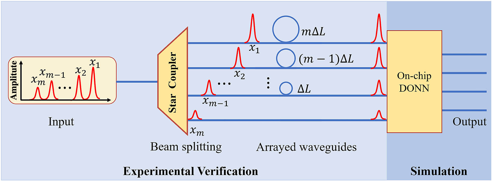
Fig. 1. Schematic diagram of converting a serial input signal into a parallel signal at a certain time using the space-time conversion method and feeding it into the on-chip DONN.
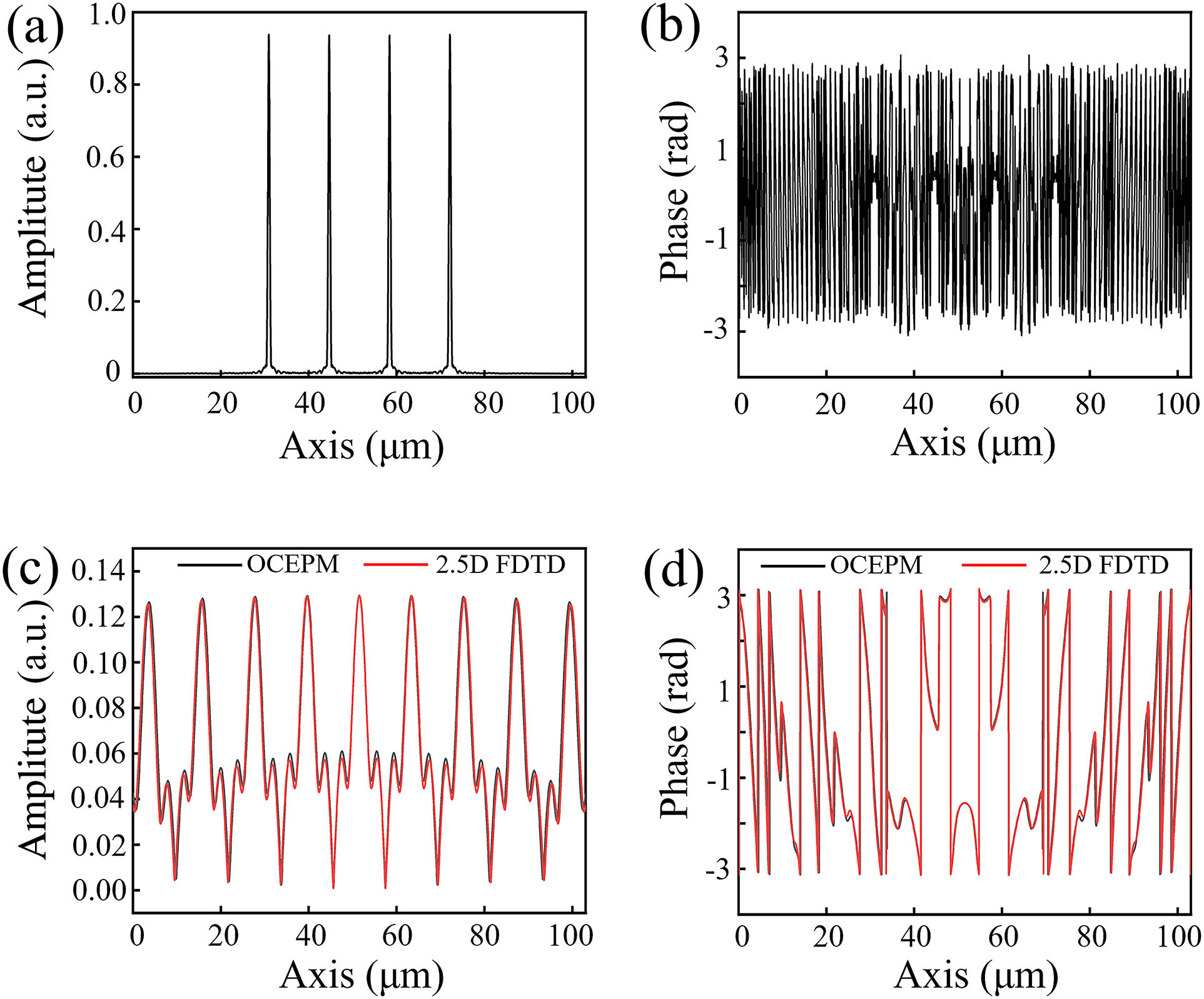
Fig. 2. (a) and (b) are the field intensity and phase distribution of the input signal, respectively. (c) and (d) are the field intensity and phase distribution of the input signal propagating 300 µm later in a slab waveguide (thickness is 220 nm, width is 105 µm) of the modified OCEPM (black line) and the 2.5D FDTD (red line), respectively.
Fig. 3. (a) Weights of neurons on the two hidden layers of the on-chip DONN designed for the vowel recognition task. (b) The schematic of the on-chip DONN. Each diffractive unit on a given layer acts as a secondary source of a wave. Each diffractive unit is a slot group composed of three identical silicon slots filled with silicon dioxide and represents a single neuron in the DONN system. (c) Logic diagram of (b), which mathematically describes the physical calculation process of the on-chip DONN. W (k) represents the kth diffraction matrix derived from the on-chip electromagnetic propagation model [Eq. (2 )]. (x1, x2, x3, x4) is the input and (y1, y2, y3, y4) is the output.
Fig. 4. (a) Loss curve on the training set (black line) and accuracy curve on the blind testing set (red line) for the optimized on-chip DONN during the learning procedure. (b) The confusion matrix by numerical calculation for the blind testing sets. (c)–(f) The display of the on-chip DONN classification results of the different types of vowel phonemes “hid”, “hEd”, “hYd”, and “hOd”, respectively.
Fig. 5. (a) Microscopic view of the fabricated arrayed waveguides. (b) Vertically coupled grating. (c) Local close-up of the vertically coupled grating. (d) Ring delay line. (e) Local close-up of the ring delay line.
Fig. 6. (a) Serial input signals. (b) The output result of the serial input signals after passing through the arrayed waveguides.
Fig. 7. (a) System experimental setup. Four chronological Gaussian pulses (S1, S2, S3, and S4) with different amplitudes generated by an arbitrary waveform generator (AWG) are loaded on the continuous-wave laser through the amplitude modulator (AM). The time slot of the input signal pulse is 100 ps corresponding to the calculated time delay. Then, the input signals with various amplitudes are coupled into the on-chip arrayed waveguides from the four vertically coupled gratings by a 1 × 4 fiber star-coupler (SC) outside the chip. Next, the serial signals in chronological order will exist in parallel at a certain moment on the output interface through the fixed true-delay lines owned by the on-chip arrayed waveguides. Ultimately, after the required parallel signals enter the on-chip DONN to complete the inference calculation, its output optical field will be coupled into the single-mode waveguides through the corresponding inverse tapers at the DONN output interface and received by the on/off-chip photodetector (PD). At this time, a classification task is completed. PC, polarization controller; Amp, electric amplifier; VOA, variable optical attenuator (which is to compensate the fabricating error of the on-chip delay lines); VODL, variable optical delay line; OSC, digital oscilloscope.
|
Table 1. Comparison between the Proposed on-Chip DONN and Other Integrated Works

Set citation alerts for the article
Please enter your email address
© Copyright 2018-2021 | Chinese Laser Press. All Rights Reserved 沪ICP备15018463号-20