
Tingzhao Fu, Yuyao Huang, Run Sun, Honghao Huang, Wencan Liu, Sigang Yang, Hongwei Chen. Integrated diffractive optical neural network with space-time interleaving[J]. Chinese Optics Letters, 2023, 21(9): 091301
- Chinese Optics Letters
- Vol. 21, Issue 9, 091301 (2023)
Abstract
1. Introduction
Artificial neural networks (ANNs) have received significant attention in many fields, including computer vision[1], natural language processing[2], decision-making[3,4], etc. Faced with complex tasks, the requirements of ANNs for computing power are more stringent, causing a heavy computation burden in existing electronic computing hardware[5–13] [e.g., the central processing unit (CPU), the graphical processing unit (GPU), the field-programmable gate array (FPGA), and the application-specific integrated circuit (ASIC)]. Therefore, an alternative novel computing architecture is imperative for performing heavy computation. Presently, optical neural networks (ONNs) have garnered tremendous interest[14–34] because of the advantages of their low power consumption, low latency, and ultrahigh bandwidth, which may solve the dilemma that the existing electronic computing architectures face.
The ONNs based on diffractive surfaces in free space can optically perform inference tasks[15,35,36], this kind of ONNs is not limited by high input dimensions. However, the ONNs based on spatial diffraction are often composed of discrete devices, such as 3D-printed metasurfaces, digital micromirror devices (DMDs), and spatial light modulators (SLMs), which are bulky and low in integration. Moreover, the unavoidable calibration process between the discrete devices may bring potential errors to the system. Consequently, these problems may limit the application scenarios of such kinds of ONNs to some extent. The ONNs based on the silicon-on-insulator (SOI) platform not only have the advantages of low power consumption, low latency, and ultrahigh computing bandwidth but also have the characteristics of small volume, light weight, good stability/portability, and unnecessary physical alignment process. There are several different implementations of the integrated ONNs, including a coherent approach based on Mach–Zehnder interferometer (MZI) mesh[14,20,21,27], wavelength-division multiplexing (WDM) processing with micro-ring resonators (MRRs), programmable routing enabled by a phase-change material (PCM)[16], and an on-chip diffractive approach based on sub-wavelength structures[17,18,29]. Among them, the ONNs designed based on MZIs, WDM-MRRs, and PCM have low integration, which makes achieving large-scale expansion difficult. The on-chip DONNs based on sub-wavelength structures can achieve high integration and large computational capacity. However, its massively parallel inputs are limited by the energy consumption and high speed. Therefore, it is significantly urgent to solve the limited input dimensions of the on-chip DONNs.
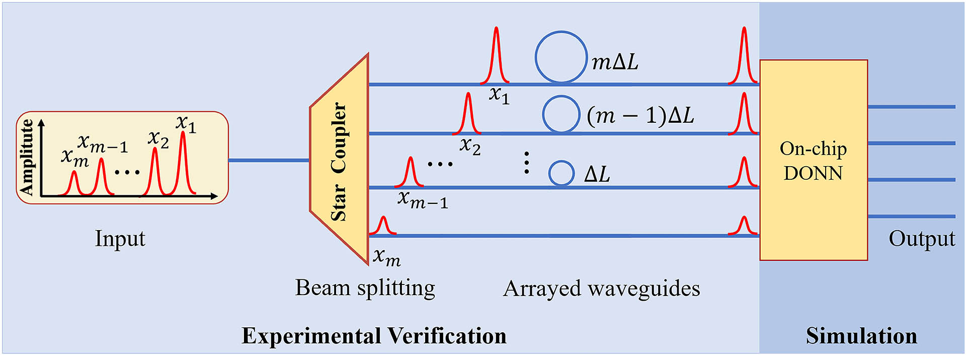
The calculation function of the DONNs is based on the mutual interference between the parallel input signals. Therefore, it must be ensured that the modulated signals enter the input section of the DONNs at the same time. Routinely, the parallel input signals can be realized by integrated phase shifters (i.e., the integrated heaters) on each waveguide[14,30,31,37]. However, it is inevitably necessary to continuously provide additional energy to maintain the normal operation of these shifters by this way. Thus, the on-chip power consumption would increase dramatically with the increase of the input dimensions. In this work, the parallel input multiple signals are realized by designing the true-delay lines of the arrayed waveguides. The interval length between the adjacent waveguides is determined by the time interval between the serial signals. The shorter the time interval, the smaller the length difference between two adjacent arrayed waveguides. Here, an on-chip DONN for the task of vowel recognition was theoretically verified, and the arrayed waveguides with different lengths were fabricated using electron beam lithography (EBL) technology based on an SOI platform. According to the modulation rate (10 Gbps), the interval difference between adjacent waveguides was set to 7.1429 mm corresponding to a 100 ps time delay. We fabricated the arrayed waveguides with a fixed length difference and experimentally demonstrated its performance. Based on the results of the fabricated arrayed waveguides, an on-chip DONN with two hidden layers (each with 70 neurons) is proposed, and the numerical calculation result of the blind test prediction of the vowel recognition dataset[38] is 98.3%. The aforementioned method for designing the on-chip DONN based on the standard complementary metal-oxide semiconductor (CMOS) process provides a solution for high dimensional inputs, low power consumption, and large capacity computing, which paves a way for promoting the applications of the on-chip DONN in various aspects.
Sign up for Chinese Optics Letters TOC. Get the latest issue of Chinese Optics Letters delivered right to you!Sign up now
2. Concept and Principle
2.1. Arrayed waveguides
The design of the arrayed waveguides is key to realizing the high dimensional parallel loading of signals using the space-time interleaving method. In Fig. 1, the length of is determined by the modulation rate of the input signal, which can be calculated by
![]()
Figure 1.Schematic diagram of converting a serial input signal into a parallel signal at a certain time using the space-time conversion method and feeding it into the on-chip DONN.
2.2. On-chip electromagnetic propagation model
In this work, an on-chip electromagnetic propagation model (OCEPM) is proposed by modifying the Huygens–Fresnel principle under restricted propagation conditions, which is shown as follows:
![]()
Figure 2.(a) and (b) are the field intensity and phase distribution of the input signal, respectively. (c) and (d) are the field intensity and phase distribution of the input signal propagating 300 µm later in a slab waveguide (thickness is 220 nm, width is 105 µm) of the modified OCEPM (black line) and the 2.5D FDTD (red line), respectively.
3. Methods
3.1. Device fabrication
The arrayed waveguides were fabricated on an SOI (100 substrate) platform with a 220-nm-thick silicon (Si) top layer and a 3-μm-thick buried oxide layer. The fiber-grating coupler loss was optimized to 5 dB per input/output facet.
3.2. Optical measurements
A continuous-wave tunable semiconductor laser with a polarization controller was used to launch light onto the chip (32 mW). The output was monitored using two dual-channel optical power meters, and the minimum power detection limit was . An external auxiliary circuit was provided by a direct current (DC) dual-tracking voltage-stabilizing source (DH1718E-5, 0–35 V).
3.3. Numerical simulations
The training process of the vowel recognition classification was conducted in Pytorch, which is a package for Python. The light diffraction connection in the process of forward and error backward propagation followed the modified Huygens–Fresnel principle. The data in the vowel recognition dataset were encoded onto the amplitude of light.
4. Numerical Calculation and Experiment
4.1. Structure design
Combining forward propagation, error backpropagation, and gradient descent algorithms, the structural parameters of an on-chip DONN can be obtained by pre-training through a computer in advance based on the OCEPM[18,39]. An on-chip DONN with two hidden layers is proposed, and the weight parameters on two hidden layers (HLs) are trained on the premise of fixing the super parameters of the DONN. The weight parameters on each HL obtained in the pre-training process, which are displayed in the form of pixels, as shown in Fig. 3(a), can be equivalently mapped onto the light in the form of the phase difference. The phase difference is realized by the optical path interval generated by the light passing through the slot group (composed of identical silicon slots filled with silicon dioxide) with different lengths. The length of the identical silicon slots in the slot group filled with silicon dioxide is calculated by
![]()
Figure 3.(a) Weights of neurons on the two hidden layers of the on-chip DONN designed for the vowel recognition task. (b) The schematic of the on-chip DONN. Each diffractive unit on a given layer acts as a secondary source of a wave. Each diffractive unit is a slot group composed of three identical silicon slots filled with silicon dioxide and represents a single neuron in the DONN system. (c) Logic diagram of (b), which mathematically describes the physical calculation process of the on-chip DONN.
In Fig. 3(b), the length of the HLs was 105 µm along the -axis. Each HL contained 70 neurons, and each value of the neurons is mapped by a slot group (consisting of three identical silicon slots filled with silicon dioxide). The center distance between the adjacent silicon slot filled with silicon dioxide (SSSD) is 500 nm, the period of the slot group is 1.5 µm, the width of the SSSD is 200 nm, and the thickness of the SSSD is 220 nm. The distance between two successive HLs was 300 µm along the -axis. In addition, the input features are loaded onto the corresponding input single-mode waveguides and propagate directly into the slab waveguide, and then propagate 300 µm through the slab waveguide to reach the first HL. After light exits the last HL, it also propagates 300 µm until it reaches the output layer of the network, with four detector regions “” () arranged in the output section. Each output detector region is assigned a specific category. The width of each detector region was 8 µm, and the distance between the centers of the two neighboring detector regions was 8 µm. Therefore, for the designed on-chip DONN, the footprint of the on-chip DONN can be calculated as . The physical calculation process can be mathematically described in Fig. 3(c), and its specific formula expression is shown in Eq. (4), where “” represents the matrix transpose. Our previous research[18,39] outlined the specific and detailed design method of the on-chip DONN structure.
4.2. Numerical calculation
In this work, an on-chip DONN for the task of vowel recognition is proposed. Meanwhile, the vowel recognition data is obtained from the pronunciation of 10 types of letters by 90 different people, here, 4 types of phonemes are selected as the classification prediction categories, namely “hid”, “hEd”, “hYd”, and “hOd”. Therefore, there is a total of 360 sets of data, which is divided into a training set and a testing set by 1:1, that is, the training set and testing set have 180 sets of data, respectively. In addition, the features of the vowel recognition dataset are compressed into four features through a fully connected layer network. Then, these features are mapped onto the amplitude of light. Based on the OCEPM, the on-chip DONN with two HLs was optimized and used for classification on the vowel recognition dataset. Figure 4(a) shows the loss values for the training set and the accuracy values for the blind testing set during the learning procedure. The confusion matrix for the blind testing set in the numerical calculation is depicted in Fig. 4(b), and the prediction accuracy is 98.3%. The recognition results of the phonemes “hid”, “hEd”, “hYd”, and “hOd” are shown in Figs. 4(c), 4(d), 4(e), and 4(f), respectively.
![]()
Figure 4.(a) Loss curve on the training set (black line) and accuracy curve on the blind testing set (red line) for the optimized on-chip DONN during the learning procedure. (b) The confusion matrix by numerical calculation for the blind testing sets. (c)–(f) The display of the on-chip DONN classification results of the different types of vowel phonemes “hid”, “hEd”, “hYd”, and “hOd”, respectively.
4.3. Experimental verification of space-time conversion performance
To verify the performance of the space-time conversion of the arrayed waveguides, four single-mode waveguides with fixed delay lines were fabricated using EBL technology based on an SOI platform, which is shown in Fig. 5. The incremental length of the fixed delay line is calculated based on Eq. (1), which is 7.1429 mm, corresponding to a 100 ps time delay.
![]()
Figure 5.(a) Microscopic view of the fabricated arrayed waveguides. (b) Vertically coupled grating. (c) Local close-up of the vertically coupled grating. (d) Ring delay line. (e) Local close-up of the ring delay line.
In this experiment, four chronological Gaussian pulses with different amplitudes generated by an arbitrary waveform generator (AWG) are loaded on the continuous-wave laser through the amplitude modulator (AM). The time slot of the input signal pulse is 100 ps, corresponding to the calculated time delay. Then, the input signals are coupled into the on-chip arrayed waveguides from the four vertically coupled gratings by a fiber star-coupler outside the chip. Ultimately, the serial signals in chronological order appear simultaneously at a certain moment on the output interface through the fixed true-delay lines owned by the on-chip arrayed waveguides. Figure 6(a) is a serial input signal, and Fig. 6(b) shows the output result of the serial input signal appearing at 626.15 ps simultaneously after passing through the arrayed waveguides, which proves that the designed arrayed waveguides with true-delay lines can achieve better space-time conversion function. Meanwhile, in Fig. 5, before compensating for losses, the losses of the arrayed waveguides from bottom to top were 15.38, 17.93, 22.03, and 25.2 dB, respectively.
![]()
Figure 6.(a) Serial input signals. (b) The output result of the serial input signals after passing through the arrayed waveguides.
4.4. System experimental implementation
In this work, we designed a system experimental setup (Fig. 7) based on the experimental verification results of arrayed waveguides and theoretically implemented the numerical calculation of the on-chip DONN. When the serial input signals pass through the designed arrayed waveguides with a fixed true-delay line, they will appear simultaneously in the input interface of the on-chip DONN in parallel at a certain moment. Based on the input of the parallel signals at that time, the on-chip DONN will perform inference calculations according to the characteristics of the input signals and give calculation results at a specific time on the output interface of the on-chip DONN. The intensity of different light field distributions on the output interface of the on-chip DONN is coupled into the single-mode waveguide through an inverse taper and then collected by a high-speed photodetector from the vertical coupling grating. Finally, the eventual classification results are given in the form of light intensity. As for the research on on-chip DONNs, related theoretical simulations[17,18,33] and experimental verifications[29,39] have been conducted.
![]()
Figure 7.(a) System experimental setup. Four chronological Gaussian pulses (S1, S2, S3, and S4) with different amplitudes generated by an arbitrary waveform generator (AWG) are loaded on the continuous-wave laser through the amplitude modulator (AM). The time slot of the input signal pulse is 100 ps corresponding to the calculated time delay. Then, the input signals with various amplitudes are coupled into the on-chip arrayed waveguides from the four vertically coupled gratings by a 1 × 4 fiber star-coupler (SC) outside the chip. Next, the serial signals in chronological order will exist in parallel at a certain moment on the output interface through the fixed true-delay lines owned by the on-chip arrayed waveguides. Ultimately, after the required parallel signals enter the on-chip DONN to complete the inference calculation, its output optical field will be coupled into the single-mode waveguides through the corresponding inverse tapers at the DONN output interface and received by the on/off-chip photodetector (PD). At this time, a classification task is completed. PC, polarization controller; Amp, electric amplifier; VOA, variable optical attenuator (which is to compensate the fabricating error of the on-chip delay lines); VODL, variable optical delay line; OSC, digital oscilloscope.
5. Discussion
5.1. Computation speed and energy efficiency
The proposed on-chip DONN architecture has the potential to process high-dimensional big data at high speeds and low power consumption. Once all the parameters have been trained and mapped onto the physical structures, the whole computing procedure is performed optically in a passive manner. Assuming that the loading signal modulation rate is Gbps, the input signal is vector in parallel after the arrayed waveguides with a fixed delay on the DONN input interface. The on-chip DONN has neurons at each HL, implementing layers of the matrix multiplication and operating at a GHz photodetection rate. The number of floating-point operations per second (FLOPS) to match the optical network is obtained using the following equation[14]:
5.2. Performance of proposed DONN framework
Recently, certain research on integrated ONNs has been conducted. Table 1 compares the proposed on-chip DONN with other integrated DONNs and ONNs. It is not difficult to find that the computing unit of on-chip DONNs is a sub-wavelength structure. Thus, its integration degree is higher than that of other on-chip ONNs. In addition, the signal loading method of the arrayed waveguides is all passive. Thus, the energy consumption only spends on the single modulator, and the energy consumption during the signal loading part would not increase with the increase of input dimensions. However, the other signal loading methods are very limited by energy consumption when dealing with high dimensional tasks because the energy consumption would increase sharply with the increase of the number of phase shifters used for signal loading.
| Study | Computing Unit | Signal Loading Method | Signal Loading Rate | On-Chip Power Consumption |
|---|---|---|---|---|
| Ref. [ | Mach-Zehnder interferometer (MZI) | Multiple thermo-optic phase shifter (MTPS) | ∼ Kbps | 1.92 W |
| Ref. [ | MZI | MTPS | ∼ Kbps | 3.92 W |
| Ref. [ | MZI | MTPS | ∼ Kbps | 7.7 mW |
| Ref. [ | Multimode interferometer | MTPS | ∼ Kbps | 2.04 W |
| Ref. [ | Subwavelength unit (SWU) | DMD and Lens group | ∼ Kbps | Passive |
| Ref. [ | SWU | MTPS | ∼ Kbps | 120 mW |
| This work | SWU | Arrayed waveguides | ∼ 1.4 Gbps | Passive |
Table 1. Comparison between the Proposed on-Chip DONN and Other Integrated Works
6. Conclusion
A wholly passive optical on-chip DONN based on an SOI platform was proposed. The signal loading method of the proposed on-chip DONN is achieved using the arrayed waveguides, which can convert the serial input signals in chronological order into parallel signals at a certain time and feed them into the on-chip DONN. The advantage of this approach is that it overcomes the problem of the existing integrated ONNs, which are limited in the input of high-dimensional signals. In addition, the conversion of serial signals to parallel signals using space-time interleaving would not consume more energy because the whole conversion process is passive. The proposed method would make the on-chip DONNs more widely applicable and may, to a certain extent, promote the further development of silicon-based photon computing.
References
[6] M. B. Taylor. The evolution of bitcoin hardware. Computer, 50, 58(2017).
[13] A. Shafiee, A. Nag, N. Muralimanohar, R. Balasubramonian, J. P. Strachan, M. Hu, R. S. Williams, V. Srikumar. ISAAC: a convolutional neural network accelerator with in-situ analog arithmetic in crossbars. ACM/IEEE 43rd Annual International Symposium on Computer Architecture (ISCA)(2016).
[37] X. Zhao, H. Lv, C. Chen, S. Tang, X. Liu, Q. Qi. On-chip Reconfigurable Optical Neural Networks(2021).
[38] D. H. Deterding. Speaker Normalisation for Automatic Speech Recognition(1990).

Set citation alerts for the article
Please enter your email address
© Copyright 2018-2021 | Chinese Laser Press. All Rights Reserved 沪ICP备15018463号-20