
Xiang Wen, Ke Xu, Qinghai Song. Design of a barcode-like waveguide nanostructurefor efficient chip–fiber coupling[J]. Photonics Research, 2016, 4(6): 209
- Photonics Research
- Vol. 4, Issue 6, 209 (2016)
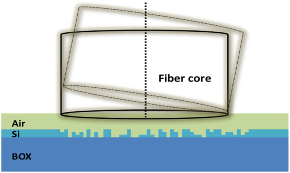
Fig. 1. Side-view schematic of the proposed discretized nanostructure.
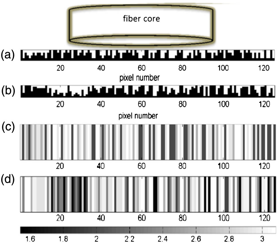
Fig. 2. Side-view schematics of the optimized coupling nanostructures for (a) four levels and (b) eight levels. Gray-scale representations of the discretized effective indices of the (c) four-level and (d) eight-level vertical coupling nanostructures.
Fig. 3. (a) Simulated amount of light leakage to the substrate. (b) Backreflection of the designed nanostructure. (c) Coupling efficiency of the two types of nanostructure.
Fig. 4. Simulated optical field distribution of the diffracted wave for the (a) four-level and (b) eight-level nanostructures, respectively.
Fig. 5. (a) Side-view schematic of the optimized eight-level polarization-independent nanostructure. Gray-scale representations of the discretized effective indices of the optimized structure for (b) TM and (c) TE.
Fig. 6. (a) Simulated amount of light leakage to the substrate. (b) Backreflections of the TE and TM modes from structure to waveguide. (c) Coupling efficiencies of the TE- and TM-mode light coupling from waveguide to single-mode fiber in the polarization-independent nanostructure.
Fig. 7. Diffractive electric field of the eight-level structure for (a) TE and (b) TM polarization.

Set citation alerts for the article
Please enter your email address
© Copyright 2018-2021 | Chinese Laser Press. All Rights Reserved 沪ICP备15018463号-20