Memoona Qammar, Bosen Zou, Jonathan E. Halpert. Organic-inorganic halide perovskites for memristors[J]. Journal of Semiconductors, 2023, 44(9): 091604
Search by keywords or author
- Journal of Semiconductors
- Vol. 44, Issue 9, 091604 (2023)
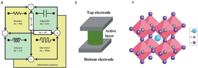
![(Color online) (a) The basic four elements of an electrical circuit. Reproduced with permission from Ref. [3]. Copyright 2008, Nature publisher. (b) MIM structure of a memristor. (c) ABX3 structure of perovskite (A and B: cations and X: anion). Reproduced with permission from Ref. [18]. Copyright 2014, Nature publisher.](/richHtml/jos/2023/44/9/091604/jos_44_9_091604_f1.jpg)
Fig. 1. (Color online) (a) The basic four elements of an electrical circuit. Reproduced with permission from Ref. [3]. Copyright 2008, Nature publisher. (b) MIM structure of a memristor. (c) ABX3 structure of perovskite (A and B: cations and X: anion). Reproduced with permission from Ref. [18]. Copyright 2014, Nature publisher.
![(Color online) Different switching mechanisms in OHP memristors. (a) Iodide vacancies are arbitrarily distributed. (b) Iodide vacancies aligned under influence of applied voltage. Inset: Movement of vacancies along the octahedral edge of structure. Reproduced with permission from Ref. [23]. Copyright 2016, American Chemical Society. (c) Architecture of Ag/MAPbI3/Ag device. (d) SEM micrograph showing 1−4 positions for EDS analysis. (e) EDS spectrum of device at LRS showing Pb and I peak intensities at four different positions shown in SEM image. Reproduced with permission from Ref. [24]. Copyright 2017, WILEY. Steps of RS via double-filament model in the Ag/MAPbI3/FTO memory device. (f) The initial state (HRS), (g) forming, (h) SET (LRS), and (i) RESET process of the device with thick MAPbI3 layer. (j) The initial state, (k) forming, (l) SET, and (m) RESET process of the device with relatively thinner MAPbI3. Reproduced with permission from Ref. [29]. Copyright 2016, American Chemical Society. (n) Mechanism of electrical switching (Ⅰ) initial state corresponding to HRS: hole trapping centres locate at the perovskite surface; (Ⅱ) SET process: Hole trap states are filled, shifting the Fermi level to the valence band; (Ⅲ) remove light electricity: a lowered barrier and quasi ohmic contact are resulted corresponding to LRS; and (Ⅳ) electrical reset: Holes are extracted from the trap states and a transition from LRS to HRS occurs. Reproduced with permission from Ref. [30]. Copyright 2018, WILEY.](/richHtml/jos/2023/44/9/091604/jos_44_9_091604_f2.jpg)
Fig. 2. (Color online) Different switching mechanisms in OHP memristors. (a) Iodide vacancies are arbitrarily distributed. (b) Iodide vacancies aligned under influence of applied voltage. Inset: Movement of vacancies along the octahedral edge of structure. Reproduced with permission from Ref. [23]. Copyright 2016, American Chemical Society. (c) Architecture of Ag/MAPbI3/Ag device. (d) SEM micrograph showing 1−4 positions for EDS analysis. (e) EDS spectrum of device at LRS showing Pb and I peak intensities at four different positions shown in SEM image. Reproduced with permission from Ref. [24]. Copyright 2017, WILEY. Steps of RS via double-filament model in the Ag/MAPbI3/FTO memory device. (f) The initial state (HRS), (g) forming, (h) SET (LRS), and (i) RESET process of the device with thick MAPbI3 layer. (j) The initial state, (k) forming, (l) SET, and (m) RESET process of the device with relatively thinner MAPbI3. Reproduced with permission from Ref. [29]. Copyright 2016, American Chemical Society. (n) Mechanism of electrical switching (Ⅰ) initial state corresponding to HRS: hole trapping centres locate at the perovskite surface; (Ⅱ) SET process: Hole trap states are filled, shifting the Fermi level to the valence band; (Ⅲ) remove light electricity: a lowered barrier and quasi ohmic contact are resulted corresponding to LRS; and (Ⅳ) electrical reset: Holes are extracted from the trap states and a transition from LRS to HRS occurs. Reproduced with permission from Ref. [30]. Copyright 2018, WILEY.
Fig. 3. (Color online) High and low resistance states of MBI ReRAM under influence of 10 ns, (a) 10 V writing pulse, (b) -10 V erasing pulse. Insets show the incident writing and erasing voltage pulse. Reproduced with permission from Ref. [36]. Copyright 2021, Royal Society of Chemistry. (c) Schematic illustration of biological (top) and artificial (bottom) nociceptor. Reproduced with permission from Ref. [49]. Copyright 2023, American Chemical Society. RS trend in EGaIn/MAPbI3/PEDOT: PSS/ITO (d) SET process and (e) RESET process in dark and in presence of different wavelengths: 636, 588, 507, and 445 nm. Insets show the logarithmic scales of the same processes. (f) Power consumption for SET, RESET and total power consumption under the influence of different light signals. Reproduced with permission from Ref. [17]. Copyright 2023, WILEY.
Fig. 4. (Color online) Material characterization of FAPbBr3. (a) XRD, (b) UV-VIS and PL spectra, (c) SEM micrograph, (d) device design, (e) RS cycles for as fabricated device, and (f) conductive mechanism via measured and fitted curve for SET state.
Fig. 5. (Color online) (a) Transmission spectra of pristine PMMA film and MAPbBr3 QDs with a complete device shown in inset. (b) RS cycles of MAPbBr3 QDs based memristor. Reproduced with permission from Ref. [42]. Copyright 2017, AIP Publishing. (c) Device architecture of MAPbI3 QWs/NWs on PET substrate with an enlarged view of QW sandwiched between Ag and Au and crystal structure of MAPbI3. Reproduced with permission from Ref. [50]. Copyright 2021, American Chemical Society.
|
Table 1. Summary of device performances of some OHP based memristors.

Set citation alerts for the article
Please enter your email address


