
Yifan Li, Yating Zhang, Zhiliang Chen, Qingyan Li, Tengteng Li, Mengyao Li, Hongliang Zhao, Quan Sheng, Wei Shi, Jianquan Yao. Self-powered, flexible, and ultrabroadband ultraviolet-terahertz photodetector based on a laser-reduced graphene oxide/CsPbBr3 composite[J]. Photonics Research, 2020, 8(8): 1301
- Photonics Research
- Vol. 8, Issue 8, 1301 (2020)
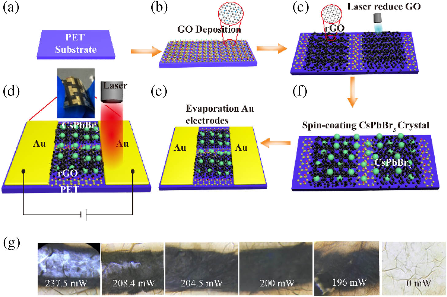
Fig. 1. (a)–(e) Processing procedures of the LSG / CsPbBr 3 LSG / CsPbBr 3 10 × 40
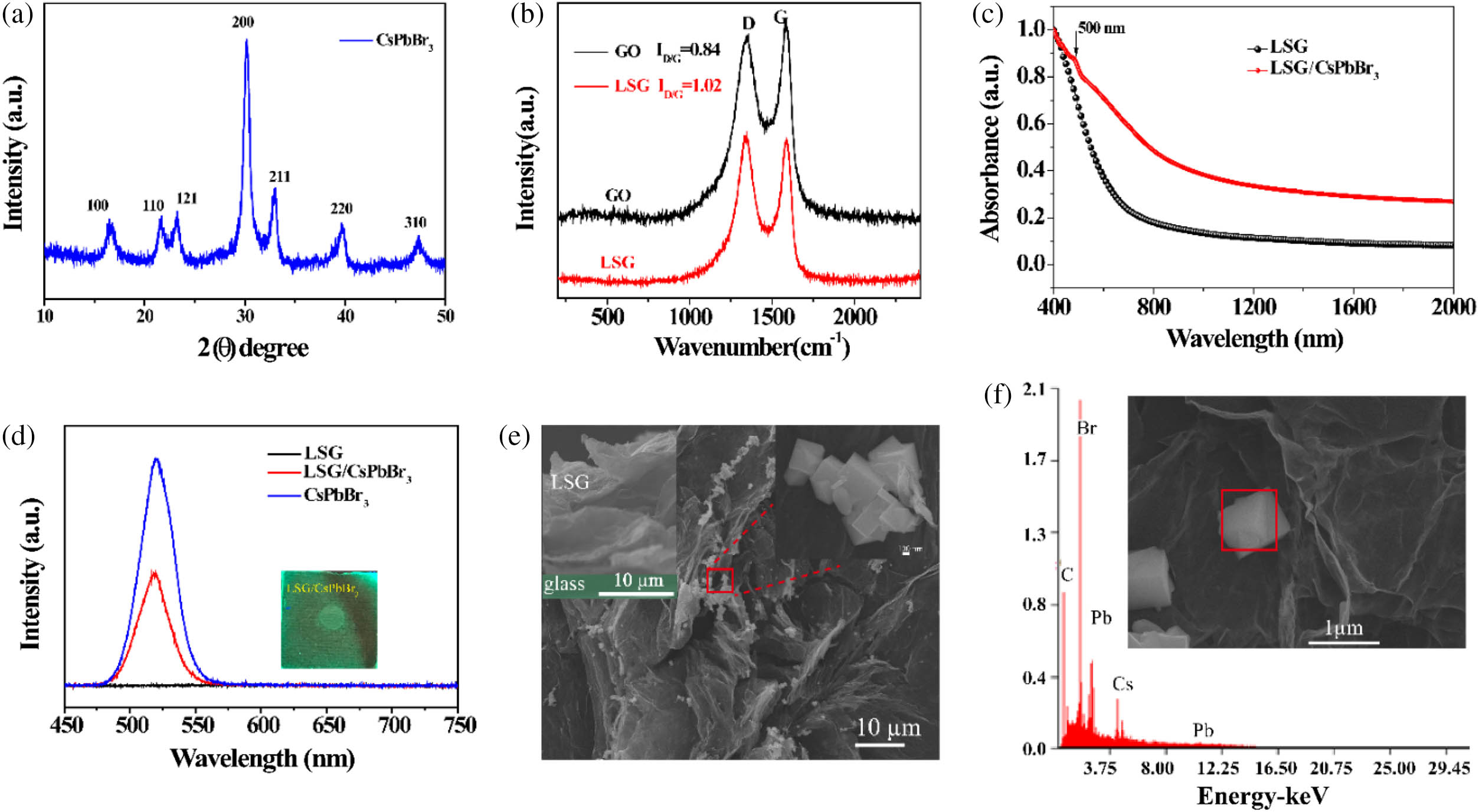
Fig. 2. (a) XRD pattern of the CsPbBr 3 LSG / CsPbBr 3 LSG / CsPbBr 3 CsPbBr 3 LSG / CsPbBr 3 LSG / CsPbBr 3
Fig. 3. (a), (b) Photocurrent voltage ( I – V ) LSG / CsPbBr 3 LSG / CsPbBr 3 932.48 mW / cm 2
Fig. 4. Optical-electrical response characteristics of the LSG / CsPbBr 3 E e LSG / CsPbBr 3 D * E e
Fig. 5. (a) Temporal photocurrent responses of the LSG device under 1064 and 1177 nm illumination at 390 mW / cm 2 390 mW / cm 2 LSG / CsPbBr 3 390 mW / cm 2 LSG / CsPbBr 3 390 mW / cm 2 R
Fig. 6. (a) Mechanism schematic for PTE effect; (b) schematic of photocurrent generation process of the device; (c) temperature profile of active location under dark and 532 nm illumination; inset, infrared imaging temperature distribution map of the device under 532 nm illumination; (d) increased temperature profile of the device under 532 nm laser illumination; (e), (f) current voltage ( I – V )
Fig. 7. (a) I – V LSG / CsPbBr 3 ( E e = 58.28 mW / cm 2 ) LSG / CsPbBr 3 ( E e = 58.28 mW / cm 2 )
|
Table 1. Optoelectronic Characteristics of Typical Photodetectors Based on Graphene and Other 2D/3D Materials

Set citation alerts for the article
Please enter your email address
© Copyright 2018-2021 | Chinese Laser Press. All Rights Reserved 沪ICP备15018463号-20