• Chinese Optics Letters
  • Vol. 19, Issue 6, 060006 (2021)
Renyou Ge1, Hao Li1, Ya Han1, Lifeng Chen1, Jian Xu2, Meiyan Wu3, Yongqing Li4, Yannong Luo5、*, and Xinlun Cai1
Author Affiliations
  • 1State Key Laboratory of Optoelectronic Materials and Technologies, School of Electronics and Information Technology, Sun Yat-sen University, Guangzhou 510275, China
  • 2School of Economics and Commerce, South China University of Technology, Guangzhou 510640, China
  • 3Laboratory of Biomedical Photonics & Engineering, School of Basic Medical Sciences, Guangxi Medical University, Nanning 530021, China
  • 4Department of Physics, East Carolina University, Greenville, North Carolina 27858-4353, USA
  • 5Life Science Institute and Laboratory of Biomedical Photonics & Engineering, Guangxi Medical University, Nanning 530021, China
  • show less
    DOI: 10.3788/COL202119.060006 Cite this Article Set citation alerts
    Renyou Ge, Hao Li, Ya Han, Lifeng Chen, Jian Xu, Meiyan Wu, Yongqing Li, Yannong Luo, Xinlun Cai. Polarization diversity two-dimensional grating coupler on x-cut lithium niobate on insulator[J]. Chinese Optics Letters, 2021, 19(6): 060006 Copy Citation Text show less

    Abstract

    We propose and demonstrate a polarization diversity two-dimensional grating coupler based on the lithium niobate on insulator platform, for the first time, to the best of our knowledge. The optimization design, performance characteristics, and fabrication tolerance of the two-dimensional grating coupler are thoroughly analyzed utilizing the three-dimensional finite-difference time-domain method. Experimentally, -7.2 dB of coupling efficiency is achieved with 1 dB bandwidth of 64 nm. The polarization-dependent loss is about 0.4 dB around 1550 nm. Our work provides new polarization multiplexing approaches for the lithium niobate on insulator platform, paving the way for critical applications such as high-speed polarization multiplexed electro-optical modulators.

    1. Introduction

    Lithium niobate on insulator (LNOI) is emerging as a promising platform for integrated photonics thanks to its large electric-optic coefficient, strong second-order optical nonlinearity, low absorption loss, and wide transparent window (from 400 nm to 5 µm)[1]. Several fundamental photonic building blocks[25] and key functional devices have been demonstrated recently, including microring resonator[6], Fourier transform spectroscopy[7], acousto-optic modulator[8], electro-optical (EO) modulator[9,10], EO frequency comb[11], and so on.

    Despite these advances, efficient coupling between a lithium niobate (LN) chip and optical fiber is still a major challenge, mainly due to the large mode mismatch between the fiber mode (diameter of 10.4 µm) and waveguide mode[12]. As one of the most popular coupling solutions, grating couplers (GCs) have been widely adopted in silicon photonics covering testing to chip packaging, with advantages of alleviated alignment tolerance, wafer-scale testing, and avoidance of facet polishing.

    Recently, several one-dimensional (1D) GCs have been demonstrated on the LNOI platform[1322]. However, compared with another popular coupling approach of inverse taper[23,24], the coupling efficiency of the conventional GC is strongly dependent on the polarization state of the input fiber mode, which is generally unknown and unstable for telecom fibers. Although a polarization-independent 1D GC enables coupling both transverse-electrical (TE) and transverse-magnetic (TM) polarization of fiber modes simultaneously and has been proposed theoretically on the hybrid silicon/LNOI platform lately[18], the subsequent polarization rotators are still required for polarization diversity applications, because most photonic devices are only designed for the TE mode.

    The two-dimensional (2D) GC, an important building block in photonic integrated circuits (PICs) to overcome polarization-dependence issues, enables coupling between the fiber and waveguide modes (TE polarization), regardless of the fiber mode polarization. Many efforts have been devoted to improving the performance of 2D GCs on the silicon on insulator (SOI) platform, including integrating a backside metal mirror[25], optimizing the grating pattern[26], and exploiting a phase shifter in one arm[27]. For practical applications, 2D GCs have been extensively applied in silicon photonic circuits[28,29] including polarization diversity, coherent receivers, and quantum PICs, yet they have never been demonstrated on the LNOI platform.

    In this Letter, we demonstrate the first, to the best of our knowledge, 2D GC on the x-cut LNOI platform. The 2D GCs are one-step etched along with LN waveguides and 1D GCs, which significantly simplifies the fabrication and is much more cost effective. The measurement results show that a coupling efficiency of 7.2dB with 1 dB bandwidth (BW) of 64 nm is achieved. The polarization-dependent loss (PDL) is about 0.4 dB around 1550 nm.

    2. Simulation and Design

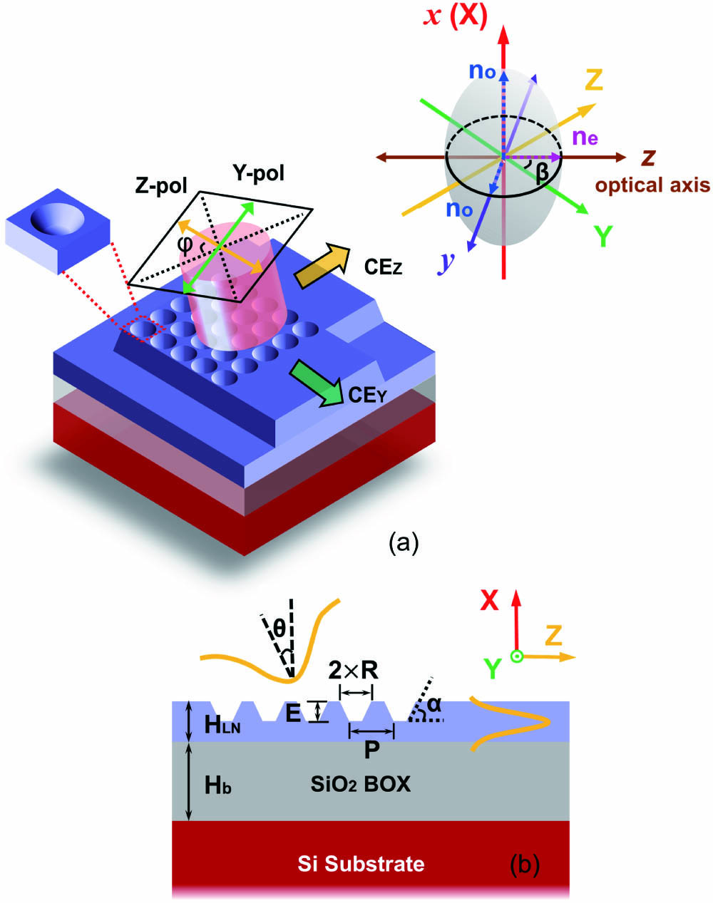
    The schematic structure of the proposed LN 2D GC is shown in Fig. 1, which is fabricated on x-cut LNOI wafers for the sake of serving LN modulators, which are mainly fabricated on x-cut LNOI wafers, benefiting from the strongest EO coefficient γ33 (27pm/V at 1500 nm), for the implementation of polarization multiplexing modulation of signals. The xyz indicates the coordinate system of LN materials with the z axis corresponding to the optical axis of the LN crystal, while the X-Y-Z represents the geometric coordinate system of the device. Two orthogonal polarization components of the fiber mode (Z polarization φ=45° and Y polarization φ=135°) are coupled into the corresponding waveguides, with coupling efficiency of CEZ and CEY, respectively. The total coupling efficiency can be defined as CET=CEZ+CEY. The cross section of the device is shown in Fig. 1(b), the thickness of the LN thin film HLN and buried oxide (BOX) layer Hb is 360 nm and 2 µm, respectively, with air cladding. The etching depth, grating pitch, and hole radius are defined as E, P, and R, which need to be further optimized. The sidewall angle of the grating is α=60°.

    (a) Schematic structure of x-cut LN 2D GCs. The angle between axis Z, Y (direction of grating) and optical axis z of LN material is β = 45°.The angle φ represents the polarization state of the fiber mode. (b) Cross-sectional view of the LN 2D GC.

    Figure 1.(a) Schematic structure of x-cut LN 2D GCs. The angle between axis Z, Y (direction of grating) and optical axis z of LN material is β = 45°.The angle φ represents the polarization state of the fiber mode. (b) Cross-sectional view of the LN 2D GC.

    Three-dimensional (3D) finite-difference time-domain (FDTD) method is utilized for the simulation. The simulation volume is 17µm×17µm×4µm, and the mesh accuracy was two in the FDTD region. An extra mesh override region of dz=dy=20nm, dx=10nm was adopted in the grating. Anisotropy of the x-cut LN thin film is taken into consideration. The design methodology is basically the same as that of SOI[30], which can be simplified into the following two steps.

    Firstly, we did a parameter sweep for E, P, and R to tune the central wavelength target on 1550 nm. In this step, the thickness of the BOX layer is fixed to Hb=2µm. As depicted in Fig. 2(a), we pick out the optimal parameter combination of R and P for each E. One can find that the highest coupling efficiency corresponds to parameters of E=220nm, P=1004nm, and R=400nm, with a coupling efficiency of 31.8% (4.98dB) at 1550 nm. However, it is more reasonable to determine the etching depth as E=180nm, considering the coupling efficiency of the 2D GC varies slightly (from 31.8% to 30.8%) when E decreases from 220 nm to 180 nm, as depicted in Fig. 2(b). Furthermore, the etching depth E=180nm is also the optimal value for optical waveguides and TE 1D GCs; therefore, the one-step etching process can be implemented, which enables an easy and cost-effective fabrication, meanwhile guaranteeing the high coupling efficiency of both 1D and 2D GCs. These advantages are appealing for polarization multiplex circuits[29], where 1D and 2D GCs need to be utilized simultaneously. Figure 2(c) presents the coupling efficiency at 1550 nm when Hb changes from 1.5 µm to 2.5 µm. One can see that the coupling efficiency varies periodically with the BOX thickness Hb, and constructive interference occurs exactly at Hb=2µm, for both the 1D GC and the 2D GC when E=180nm. The coupling efficiency can be further improved by introducing a metal reflector beneath the BOX layer[25]. The proposed wafer structure is shown in the inset of Fig. 2(d), which is commercially available. One can see that the peak coupling efficiencies are improved to 1.4dB and 2.5dB for the 1D GC and 2D GC, respectively, due to the enhanced directionality. In the following simulation, E=180nm, P=982nm, and R=400nm are selected as the optimized parameters.

    (a) Coupling efficiency of the 2D GC for different structure parameters, when HLN = 360 nm, Hb = 2 µm, θ = 10°, and α = 60°. (b) The dependence of coupling efficiency and etching depth for 1D and 2D GCs at a wavelength of 1550 nm. (c) The coupling efficiency as a function of BOX thickness Hb at 1550 nm, with the parameters E = 180 nm, P = 982 nm, and R = 400 nm for the 2D GC, and E = 180 nm, P = 1.02 µm, and no = 2.21, with a duty cycle of 0.38 for uniform 1D GCs. (d) Coupling efficiency of 1D and 2D GCs with a gold mirror when Hb = 2 µm.

    Figure 2.(a) Coupling efficiency of the 2D GC for different structure parameters, when HLN = 360 nm, Hb = 2 µm, θ = 10°, and α = 60°. (b) The dependence of coupling efficiency and etching depth for 1D and 2D GCs at a wavelength of 1550 nm. (c) The coupling efficiency as a function of BOX thickness Hb at 1550 nm, with the parameters E = 180 nm, P = 982 nm, and R = 400 nm for the 2D GC, and E = 180 nm, P = 1.02 µm, and no = 2.21, with a duty cycle of 0.38 for uniform 1D GCs. (d) Coupling efficiency of 1D and 2D GCs with a gold mirror when Hb = 2 µm.

    Secondly, we calculated the angle between two LN waveguides using a large simulation volume of 76.5µm×21µm×3µm. The two strip waveguides are replaced by an LN slab waveguide to investigate the intrinsic propagation direction of the coupled waveguide mode. As shown in Fig. 3, the coupled mode propagates and deviates about 2° from the Z axis, which means the angle of two LN strip waveguides connecting the 2D GC is 86°. It should be noted that it is feasible to transfer such a design flow to z-cut LNOI thin film, theoretically. However, the optimized structure parameters such as P and R may have a minor change due to the anisotropy of LN.

    Propagation of the coupled mode in the LN slab waveguide.

    Figure 3.Propagation of the coupled mode in the LN slab waveguide.

    To investigate the performance sensitivity of 2D GCs to the input polarization state, we calculate the coupling efficiency of CEZ, CEY, and CET as a function of polarization angle φ, as shown in Fig. 4(a). It is seen that CEZ and CEY vary from 19.1dB to 5.1dB when the polarization angle φ swept through 360°, giving an extinction ratio of 14dB. Moreover, the influence of the polarization angle on CET is relatively small, which can be expressed as CET(φ)=5.020.5cos(2φ) (dB). This indicates that the PDL is about 1 dB, the maximum CET is 4.5dB for S polarization when φ=90° and 270°, and the minimum CET is 5.5dB for P polarization when φ=0°, 180°, and 360°. Figure 4(b) illustrates the coupling spectra for the case of φ=75°, where CEY/CEZ0.383, and the 1 dB BW is 61 nm. Figure 4(c) presents the dependence of the central wavelength λc on polarization angle φ. As seen, the central wavelength λc varies slightly around the target wavelength (Δλc±9nm), which is far less than the 60 nm 1 dB BW, indicating that the influence of the polarization angle on the device performance is limited. Furthermore, we studied the fabrication tolerance of the proposed 2D GC. Figures 5(a)5(d) summarize the variations of coupling efficiency with variations of etching depth E, grating pitch P, radius of hole R, and sidewall angle α. Overall, the proposed 2D GC shows a good fabrication tolerance.

    (a) Coupling efficiency of CEZ, CEY, and CET as a function of the polarization angle φ. (b) Coupling spectra of CEZ, CEY, and CET when φ = 75°. (c) Relationship between the central wavelength λc and polarization angle φ.

    Figure 4.(a) Coupling efficiency of CEZ, CEY, and CET as a function of the polarization angle φ. (b) Coupling spectra of CEZ, CEY, and CET when φ = 75°. (c) Relationship between the central wavelength λc and polarization angle φ.

    Impact of the variation of (a) etching depth ΔE, (b) grating pitch ΔP, (c) hole radius ΔR, and (d) sidewall angle Δα.

    Figure 5.Impact of the variation of (a) etching depth ΔE, (b) grating pitch ΔP, (c) hole radius ΔR, and (d) sidewall angle Δα.

    3. Fabrication and Measurement

    The proposed devices were fabricated on a commercial 360 nm thick x-cut LNOI wafer (NANOLN). The optical waveguides and grating cells were firstly patterned by electron-beam lithography (EBL) in hydrogen silsesquioxane (HSQ) resist and then dry etched by the argon-based inductively coupled plasma (ICP) etching process. Figure 6(a) shows the scanning electron microscope (SEM) image of the fabricated 2D GC. The inset picture presents the details of the grating cells. As depicted in Fig. 6(b), one pair of 2D GCs was connected in a back-to-back configuration to measure the coupling efficiency and PDL. The 1D GCs were also fabricated on the same chip to calibrate the polarization state of input light by maximizing or minimizing transmission of the 1D GCs. As shown in Fig. 6(c), a broadband tunable laser (Venturi TLB-8800) was used as the light source. The polarization of input light is adjusted by a fiber polarization controller and two six-axis stages, enabling the fiber-to-chip alignment with high precision.

    (a) SEM image of LN 2D GCs. The inset shows the zoom-in picture of grating cells. (b) Optical image of the LN 2D GCs. (c) Experimental set-up scheme: TL, tunable laser; PC, polarization controller; PM, power meter.

    Figure 6.(a) SEM image of LN 2D GCs. The inset shows the zoom-in picture of grating cells. (b) Optical image of the LN 2D GCs. (c) Experimental set-up scheme: TL, tunable laser; PC, polarization controller; PM, power meter.

    Figure 7(a) shows the measured spectra of the fabricated 1D and 2D GCs. The peak coupling efficiency of the 1D GC is about 3.9dB, lower than the best experimental result of 1.43dB reported in Ref. [21] using chirped gratings. The 1 dB BW of the 1D GC is 63 nm. The waveguide propagation loss is about 0.5 dB/cm for the case of air cladding. The coupling efficiency of the 2D GC is about 7dB and 7.4dB at 1550 nm for S-polarized and P-polarized light at best, which is 2 dB lower than the simulated results. This is due to the fabrication imperfection, including insufficient etching depth and larger sidewall angle of holes, as indicated in Figs. 5(a) and 5(d). Some minor fluctuations (<0.2dB) can be found in the measured spectra, which is caused by the weak reflection at the interfaces between the grating region and waveguide. This effect can be eliminated or reduced by using a special design[31]. A valid way to further improve coupling efficiency of 1D and 2D GCs includes improving the mode overlap between the diffracted mode of gratings and Gaussian mode of fibers by optimizing the grating patterns and enhancing the directionality by introducing a backside metal mirror. The PDL is about 0.4 dB around 1550 nm, and the 1 dB BW is 64 nm. Figure 7(b) shows the measured coupling spectra of 2D GCs with different hole radii. One can observe a 25 nm blue shift of the central wavelength and 0.74 dB coupling efficiency improvement when R increases from 380 nm to 420 nm, which agrees well with the calculated results, as shown in Fig. 5(c).

    (a) Measured and calculated coupling efficiencies for the LN 1D GC and 2D GC. (b) Measured coupling efficiencies of the LN 2D GC with different hole radii.

    Figure 7.(a) Measured and calculated coupling efficiencies for the LN 1D GC and 2D GC. (b) Measured coupling efficiencies of the LN 2D GC with different hole radii.

    4. Conclusion

    In summary, we have demonstrated the first 2D GC on the LNOI platform. The measured coupling efficiency is 7.2dB at a wavelength of 1550 nm with 1 dB BW of 64 nm. The PDL is about 0.4 dB around 1550 nm. The devices are directly etched on LN thin film, and the 180 nm etching depth enables the best efficiency coupling for both 1D and 2D GCs. One-step etching for both GCs and waveguides significantly simplifies the fabrication process. Our work provides new polarization multiplexing approaches for the LNOI platform, which enables various critical applications including polarization multiplex EO modulators and nonlinear optical circuits, on-chip quantum polarization state preparation, and information processing.

    References

    [1] A. Boes, B. Corcoran, L. Chang, J. Bowers, A. Mitchell. Status and potential of lithium niobate on insulator (LNOI) for photonic integrated circuits. Laser Photon. Rev., 12, 1700256(2018).

    [2] L. Cai, A. Mahmoud, G. Piazza. Low-loss waveguides on Y-cut thin film lithium niobate: towards acousto-optic applications. Opt. Express, 27, 9794(2019).

    [3] M. Zhang, C. Wang, R. Cheng, A. Shams-Ansari, M. Lončar. Monolithic ultra-high-Q lithium niobate microring resonator. Optica, 4, 1536(2017).

    [4] Y. Liu, X. Huang, Z. Li, Y. Kuang, H. Guan, Q. Wei, Z. Fan, Z. Li. TE/TM-pass polarizers based on lateral leakage in a thin film lithium niobate–silicon nitride hybrid platform. Opt. Lett., 45, 4915(2020).

    [5] T. Ding, Y. Zheng, X. Chen. On-chip solc-type polarization control and wavelength filtering utilizing periodically poled lithium niobate on insulator ridge waveguide. J. Lightwave Technol., 37, 1296(2019).

    [6] J.-Y. Chen, Z.-H. Ma, Y. M. Sua, Z. Li, C. Tang, Y.-P. Huang. Ultra-efficient frequency conversion in quasi-phase-matched lithium niobate microrings. Optica, 6, 1244(2019).

    [7] D. Pohl, M. R. Escalé, M. Madi, F. Kaufmann, P. Brotzer, A. Sergeyev, B. Guldimann, P. Giaccari, E. Alberti, U. Meier, R. Grange. An integrated broadband spectrometer on thin-film lithium niobate. Nat. Photon., 14, 24(2020).

    [8] L. Cai, A. Mahmoud, M. Khan, M. Mahmoud, T. Mukherjee, J. Bain, G. Piazza. Acousto-optical modulation of thin film lithium niobate waveguide devices. Photon. Res., 7, 1003(2019).

    [9] M. Xu, M. He, H. Zhang, J. Jian, Y. Pan, X. Liu, L. Chen, X. Meng, H. Chen, Z. Li, X. Xiao, S. Yu, S. Yu, X. Cai. High-performance coherent optical modulators based on thin-film lithium niobate platform. Nat. Commun., 11, 3911(2020).

    [10] M. He, M. Xu, Y. Ren, J. Jian, Z. Ruan, Y. Xu, S. Gao, S. Sun, X. Wen, L. Zhou, L. Liu, C. Guo, H. Chen, S. Yu, L. Liu, X. Cai. High-performance hybrid silicon and lithium niobate Mach–Zehnder modulators for 100 Gbit s−1 and beyond. Nat. Photon., 13, 359(2019).

    [11] M. Zhang, B. Buscaino, C. Wang, A. Shams-Ansari, C. Reimer, R. Zhu, J. M. Kahn, M. Lončar. Broadband electro-optic frequency comb generation in a lithium niobate microring resonator. Nature, 568, 373(2019).

    [12] Y. Qi, Y. Li. Integrated lithium niobate photonics. Nanophotonics, 9, 1287(2020).

    [13] Z. Chen, Y. Ning, Y. Xun. Chirped and apodized grating couplers on lithium niobate thin film. Opt. Mater., 10, 2513(2020).

    [14] J. Jian, P. Xu, H. Chen, M. He, Z. Wu, L. Zhou, L. Liu, C. Yang, S. Yu. High-efficiency hybrid amorphous silicon grating couplers for sub-micron-sized lithium niobate waveguides. Opt. Express, 26, 29651(2018).

    [15] A. Kar, M. Bahadori, S. Gong, L. L. Goddard. Realization of alignment-tolerant grating couplers for z-cut thin-film lithium niobate. Opt. Express, 27, 15856(2019).

    [16] I. Krasnokutska, R. J. Chapman, J.-L. J. Tambasco, A. Peruzzo. High coupling efficiency grating couplers on lithium niobate on insulator. Opt. Express, 27, 17681(2019).

    [17] Y. Liu, X. Huang, Z. Li, H. Guan, Q. Wei, Z. Fan, W. Han, Z. Li. Efficient grating couplers on a thin film lithium niobate–silicon rich nitride hybrid platform. Opt. Lett., 45, 6847(2020).

    [18] X. Ma, C. Zhuang, R. Zeng, J. J. Coleman, W. Zhou. Polarization-independent one-dimensional grating coupler design on hybrid silicon/LNOI platform. Opt. Express, 28, 17113(2020).

    [19] M. S. Nisar, X. Zhao, A. Pan, S. Yuan, J. Xia. Grating coupler for an on-chip lithium niobate ridge waveguide. IEEE Photon. J., 9, 6600208(2016).

    [20] Z. Ruan, J. Hu, Y. Xue, J. Liu, B. Chen, J. Wang, K. Chen, P. Chen, L. Liu. Metal based grating coupler on a thin-film lithium niobate waveguide. Opt. Express, 28, 35615(2020).

    [21] K. Shuting, R. Zhang, Z. Hao, J. Di, F. Gao, F. Bo, G. Zhang, J. Xu. High-efficiency chirped grating couplers on lithium niobate on insulator. Opt. Lett., 45, 6651(2020).

    [22] Z. Chen, Y. Wang, Y. Jiang, R. Kong, H. Hu. Grating coupler on single-crystal lithium niobate thin film. Opt. Mater., 72, 136(2017).

    [23] I. Krasnokutska, J.-L. J. Tambasco, A. Peruzzo. Nanostructuring of LNOI for efficient edge coupling. Opt. Express, 27, 16578(2019).

    [24] L. He, M. Zhang, A. Shams-Ansari, R. Zhu, C. Wang, L. Marko. Low-loss fiber-to-chip interface for lithium niobate photonic integrated circuits. Opt. Lett., 44, 2314(2019).

    [25] Y. Luo, Z. Nong, S. Gao, H. Huang, Y. Zhu, L. Liu, L. Zhou, J. Xu, L. Liu, S. Yu, X. Cai. Low-loss two-dimensional silicon photonic grating coupler with a backside metal mirror. Opt. Lett., 43, 474(2018).

    [26] B. Chen, X. Zhang, J. Hu, Y. Zhu, X. Cai, P. Chen, L. Liu. Two-dimensional grating coupler on silicon with a high coupling efficiency and a low polarization-dependent loss. Opt. Express, 28, 4001(2020).

    [27] R. Halir, D. Vermeulen, G. Roelkens. Reducing polarization-dependent loss of silicon-on-insulator fiber to chip grating couplers. IEEE Photon. Technol. Lett., 22, 389(2010).

    [28] W. Bogaerts, D. Taillaert, P. Dumon, D. Van Thourhout, R. Baets, E. Pluk. A polarization-diversity wavelength duplexer circuit in silicon-on-insulator photonic wires. Opt. Express, 15, 1567(2007).

    [29] D. Bunandar, A. Lentine, C. Lee, H. Cai, C. M. Long, N. Boynton, N. Martinez, C. DeRose, C. Chen, M. Grein, T. Douglas, A. Starbuck, A. Pomerene, S. Hamilton, F. N. C. Wong, R. Camacho, P. Davids, J. Urayama, D. Englund. Metropolitan quantum key distribution with silicon photonics. Phys. Rev. X, 8, 021009(2018).

    [30] L. Carroll, D. Gerace, I. Cristiani, S. Menezo, L. C. Andreani. Broad parameter optimization of polarization-diversity 2D grating couplers for silicon photonics. Opt. Express, 21, 21556(2013).

    [31] Y. Wang, W. Shi, X. Wang, Z. Lu, M. Caverley, R. Bojko, L. Chrostowski, N. A. F. Jaeger. Design of broadband subwavelength grating couplers with low back reflection. Opt. Lett., 40, 4647(2015).

    Renyou Ge, Hao Li, Ya Han, Lifeng Chen, Jian Xu, Meiyan Wu, Yongqing Li, Yannong Luo, Xinlun Cai. Polarization diversity two-dimensional grating coupler on x-cut lithium niobate on insulator[J]. Chinese Optics Letters, 2021, 19(6): 060006
    Download Citation