Mohamed H. El Sherif1, Mohamed H. Bakr1,*, and Ezzeldin A. Soliman2
Abstract
In this paper we present a novel nanoantenna (nantenna) design for energy harvesting. The nantenna has an “E” shape and is placed on a SiO2 substrate. Its operation is based on the excitation of surface plasmon polaritons through the gold arms of the E shape. By varying the lengths and widths of the arms, two overlapping working bandwidths can be achieved. This results in a wideband behavior characterized by a full width at half-maximum of about 2.2 μm centered around 3.6 μm. Two orthogonal E nantennas are placed perpendicular to each other to realize a dual-polarized nantenna. This nantenna can receive the two incident polarizations at two separate gap locations with very high isolation. The proposed structure can be used in several energy harvesting applications, such as scavenging the infrared heat from the Earth and other hot objects, in addition to optical communications.crystals;Subwavelength structures, nanostructures;Resonance1. INTRODUCTION
During the past few years, the optical properties of metallic nanoparticles have been widely studied [1]. The progress in the study of metamaterials led to gaining insight into several phenomena that cannot be attained with natural materials. With the recent advances in technology, it is now possible to realize nano devices and subwavelength structures with sufficient accuracy. These structures include plasmonic devices, nanoantennas (nantennas), metamaterials, and terahertz filters. Plasmonic devices guide and manipulate light on a metal/dielectric interface. They have been used for various operations, such as 3D chips [2], power splitters [3], solar cells [4], and biosensors [5]. Plasmonic structures efficiently facilitate interactions between propagating radiation and nanoscale devices by squeezing light into subwavelength volumes [6].
Incident and reflective electromagnetic radiation originating from the Sun offers a constant energy source to Earth [7]. The energy reaching the Earth is in both the visible and the infrared regions. The reradiated infrared energy from the Earth may be harvested through nantennas. Unlike solar cells, these nantennas will not only collect the Sun’s light and convert it to energy, but will also collect infrared radiation. This will vastly improve energy harvesting techniques, as nantennas will operate all day long, and are not restricted by the presence of the Sun. By properly designing the nantenna, hot spots are formed at resonance, within which the intensity of the incident electromagnetic field is enhanced by several orders of magnitude. These resonances make it possible to build antennas operating at the visible and infrared ranges [8]. Nantennas have been also applied in a number of applications, including biosensing [5], energy harvesting [9], imaging [10], and optical storage [11].
A few nantenna geometries have been proposed for energy harvesting. These include dipole [9], crescent [12], fractal [13], composite [14], and bowtie nantennas [6]. In [12], the crescent shape of the nantenna concentrates the field in the gap between the displaced circular aperture and the circular patch. A large field intensity enhancement of 3000 is achieved. In [13] and [14], variations of the bowtie antenna were used. The Sierpiński triangle is used in [13] to construct several modifications to the bowtie nantenna, achieving an intensity enhancement of around 60 between 1.0 and 4.0 μm. In [14], a number of plasmonic dipoles with a common gap are proposed. This configuration has the ability to localize the incident light with different wavelengths with an intensity enhancement of more than 500. The achieved wideband behavior necessitates multipolarizations of the incident wave. In [15], a combination of a bowtie and a rectangular nanoaperture is used to achieve an intensity enhancement of 18,000 at optical wavelengths. However, the feature dimension of this design is very small, which increases the cost of fabrication.
Sign up for Photonics Research TOC. Get the latest issue of Photonics Research delivered right to you!Sign up now
In this paper, we propose a novel E-shaped nantenna for energy harvesting applications. The structure produces an electric field intensity enhancement of more than 5000 over a wide bandwidth of more than 2.2 μm. Moreover, the configuration is simple to fabricate using existing technology and can be easily scaled to larger wavelengths in the far-infrared region. The structure is simulated using Lumerical’s FDTD Solutions [16]. In Section 2, we introduce the new E-shaped structure and its theory of operation. Section 3 presents the spectral response of the nantenna, which is characterized by high intensity enhancement and a wide bandwidth. In Section 4, a parametric study is presented that demonstrates how the spectral response can be engineered. The dual-polarized version of the proposed nantenna is presented in Section 5, where two E-shaped nantennas are placed perpendicular to each other in order to absorb the incident electromagnetic radiation regardless of its polarization. Finally, we conclude the work in Section 6.
2. E-NANTENNA STRUCTURE
Figure 1 shows the side and top views of the proposed E-shaped nantenna structure. The nantenna is illuminated by a plane wave incident perpendicularly on the substrate with its electric field polarized along the parallel arms of the E nantenna. The spectrum of the incident radiation covers the range 1.0–6.0 μm. The nantenna is made from gold, and it is modeled using a Drude model with a relative permittivity of , a plasma oscillation frequency of , and a plasma collision frequency of . The nantenna is located on top of an infinite substrate and the background medium is assumed to be free space. It has five geometrical parameters: the lengths of the outer arms along and directions, and , respectively; the width of the outer arms, ; and the length and width of the inner arm, and , respectively, as shown in Fig. 1.
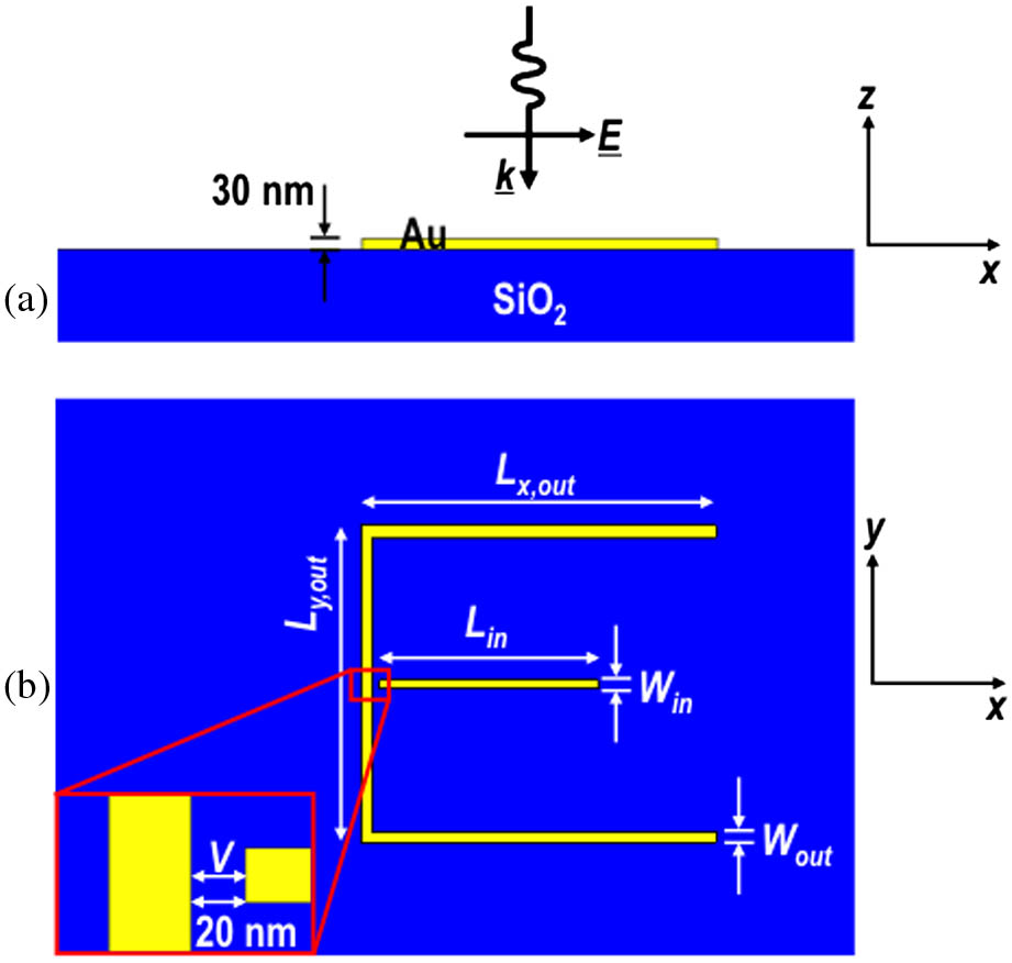
Figure 1.E-shape nantenna configuration: (a) side view and (b) top view.
The thickness of the gold layer is 30 nm. The nantenna gap has a lateral dimension of . Consequently, the hot-spot region of the proposed nantenna has dimensions of . The nantenna gap where the electric field intensity is calculated is marked with red border line in Fig. 1(b). The nantenna is modeled using Lumerical FDTD [16]. A mesh of cubic cells, , is utilized in the gap. The arms of the nantenna are meshed using mesh cells. This mesh is found suitable according to a numerical convergence test that has been performed.
The operation mechanism of the proposed nantenna can be briefly described as follows: the incident plane wave excites surface plasmon polaritons (SPPs) along the inner and outer arms of the E nantenna, as shown in Fig. 2. These waves are confined at the interfaces between the gold and the surrounding dielectric regions. The values of the resonance frequencies of the excited SPPs depend on the length of the inner and outer arms. The long outer arms support redshifted SPPs, while the short inner arm supports blueshifted SPPs, as shown in Fig. 2. The open circuit terminations of the arms result in reflected SPPs. The superposition of the incident and reflected SPPs gives rise to standing wave patterns terminated by current nulls at the locations of the open circuits. This induced current pattern is associated with induced voltage difference at the nantenna gap. If the lengths of the nantenna arms are made different from each other, two resonances occur. The parameters of the nantenna can be optimized such that the working bands around these two resonance wavelengths overlap, resulting in wideband behavior.

Figure 2.Excited SPPs along the arms of the E nantenna illuminated with a plane wave.
3. SPECTRAL RESPONSE
In this section, the spectral response of the proposed design is presented together with an illustration of the operation mechanism via field distributions. The satisfactory design should possess a spectral response with two symmetric resonances of maximum possible field intensity. The minimum intensity in between the two resonances should be slightly above half of the maximum. Satisfying this condition maximizes the full width at half-maximum (FWHM) of the nantenna. The FWHM is calculated as the difference between the two wavelengths at which the intensity enhancement is half that of the maximum. Figure 3 shows the spectral response that meets the aforementioned criterion with acceptable difference between the intensities at the two resonances. The corresponding dimensions are , , , , and . The maximum field intensity enhancement relative to the incident field is 4700 with a FWHM of 2.2 μm centered around 3.6 μm. Normalizing the FWHM with respect to the center of the bandwidth results in a percentage fractional FWHM (FFWHM) of 61%.
Figure 3.Intensity enhancement at the gap of the proposed E nantenna versus wavelength.
Figures 4(a) and 4(b) show the electric field intensity distribution along the central horizontal plane at the two resonances of 2.88 and 4.41 μm. These distributions prove that the E nantenna is capable of confining all the incident radiation at its gap, which is known as the “hot spot” of the nantenna. The size of the hot-spot region is well below the diffraction limit, which is a property of plasmonic antennas. The distributions of the normal magnetic field component along the same central horizontal plane of the nantenna are displayed in Figs. 5(a) and 5(b) at the first and second resonance wavelengths, respectively. In this figure, the red and blue indicate positive and negative values of . One can verify that the magnetic field winds itself around the short inner arm at the first resonance. The magnetic field winds itself around the long outer arm at the second resonance. Knowing that the magnetic field always circulates the electric current, it can be concluded that the second resonance wavelength is attributed to the current flowing along the outer arm. Similarly, the current flowing along the inner arm gives rise to the first resonance. Hence, the lengths of these arms ( and ) play a major role in controlling the locations of the two resonance wavelengths of the proposed E nantenna. This important conclusion is verified via the parametric study performed in the following section.
Figure 4.Electric field intensity distribution along the central plane of the E nantenna with , , , , and : (a) and (b) .
Figure 5.Distribution of the magnetic field component along the central plane of the E nantenna with , , , , and : (a) and (b) .
Figure 5 indicates that the coupling through the capacitive junction between the inner and outer arms is insignificant. At the shorter resonance wavelength, the inner arm is excited, while no excitation is transferred to the outer arm, as shown in Fig. 5(a). On the other hand, Fig. 5(b) confirms that the outer arm is excited at the longer resonance wavelength without significant excitation of the inner arm. Quantitatively, the coupling between the two arms through the capacitive junction representing the nantenna gap can be measured as shown in Fig. 6. Three modal ports are assigned to the terminals of the capacitive junction. The modal electric field distribution of the fundamental mode of a single gold rod on top of the oxide substrate is shown in the inset of Fig. 6. The S parameters describing the interaction among the three ports are plotted versus wavelength in Fig. 7. Due to symmetry and reciprocity, exciting the junction at port 1 is enough to describe all coupling mechanisms. The majority of the excitation at port 1 is transmitted to the opposite port 3, as measured by . The amount of excitation coupled to port 2, i.e., , is always less than by 7 dB. Very little energy is reflected back to port 1 as measured by . It should be noted here that the incident power should be higher than the summation of powers delivered to the three ports due to the internal losses within the gold rods. Since is much less than , it can be concluded that the capacitive coupling between the inner and outer arms is minimal.
Figure 6.Capacitive junction coupling between the inner and outer arms.
Figure 7.S parameters describing the coupling between the inner and outer arms.
The spectrum of the extinction cross section of an infinite array of the proposed E nantenna is plotted in Fig. 8. Different periodicities are considered, , 1300, and 1500 nm, where and are the and dimensions of the unit cell that is repeated periodically along the lateral plane. The extinction cross section, , is calculated through where is the transmission coefficient representing the ratio between the transmitted power density through the nantenna array to the incident power density. The double resonance behavior of the proposed nantenna can also be seen in the extinction cross-section spectrum, which confirms its wideband behavior. The level of increases as the size of the unit cell increases, which is expected. The locations of the resonance wavelengths are almost insensitive to the value of the periodicity as long as the spacing between the adjacent cells is large enough to prevent significant mutual coupling between them.
Figure 8.Extinction cross section of the E-nantenna array versus wavelength for different values of the periodicity.
4. PARAMETRIC STUDY
The selected dimensions of the proposed E nantenna for maximum bandwidth are as follows: , , , , and . These values are the coordinates of the central parameter values around which a parametric study is performed. When is increased, with all other parameters fixed, the second resonance is redshifted, as shown in Fig. 9. This is expected as is the length of the horizontal outer arms that are parallel to the incident electric field. Similarly, an increase in the less controlling parameter causes a little redshift of the second resonance, as shown in Fig. 10.
Figure 9.Intensity enhancement at the nantenna gap versus wavelength for different values of the outer arm horizontal length .
Figure 10.Intensity enhancement at the nantenna gap versus wavelength for different values of the outer arms vertical length .
An increase in the outer arm width, , causes a decrease in the effective refractive index of the SPP flowing through the outer arm. Consequently, the second resonance is blueshifted, as shown in Fig. 11. It can be concluded that the dimensions of the outer long arm affect most the second resonance. The first resonance is mainly controlled by the dimensions of the inner short arm. It behaves in the same way as the second resonance. Increases in and result in redshift and blueshift of the first resonance, as shown in Figs. 12 and 13, respectively.
Figure 11.Intensity enhancement at the nantenna gap versus wavelength for different values of outer arm width .
Figure 12.Intensity enhancement at the nantenna gap versus wavelength for different values of inner arm length .
Figure 13.Intensity enhancement at the nantenna gap versus wavelength for different values of inner arm width .
When the structure is illuminated with an -polarized wave, changing parameters in the direction, such as , , and , affect the resonance shift more than changes in other parameters. Changing -direction parameters such as and affect the intensity enhancement more than the other parameters.
5. DUAL-POLARIZED NANTENNA
Having a nantenna that can manipulate or absorb two orthogonal polarizations of the incident radiation ( and polarizations) would significantly improve the harvesting efficiency and reduce space and cost. Figure 14 shows a proposed dual-polarized version of the E nantenna. It can be looked at as two E nantennas located perpendicular to each other. The inner arms of the two E nantennas are shifted 20.0 nm above and below the outer arms to avoid their intersection, which enhances the isolation between the two polarizations. The outer arms of the two E nantennas are connected with each other to form a square ring, as shown in Fig. 14. This dual-polarized nantenna has two gaps, and , that are located between the inner arms and the ring. The locations of these gaps are shown in Fig. 14(a). Each gap receives the polarization parallel to its inner arm, where a voltage difference is induced. The spacing between the ring and the two inner arms is filled with a layer, as shown in Fig. 14(a).
Figure 14.Dual-polarized E nantenna, where the layer is drawn semi-transparent for better visibility: (a) side view and (b) top view.
To maintain symmetry with respect to the two incident polarizations, the dimensions and should be the same (). This makes the ring square in shape. The selected dimensions of the proposed dual-polarized nantenna for maximum discrimination between the two polarizations are found to be , , , and . Figures 15(a) and 15(b) show the intensity at the two gaps of the dual-polarized nantenna when illuminated with two plane waves whose electric fields are and polarized, respectively. It is clear that the cross-polarization discrimination at the two gaps is sufficiently high. Quantitatively, the ratio between the maximum wanted polarization to the maximum unwanted polarization at the two gaps is 22.8. It is worth mentioning that the maximum intensity enhancement in is slightly higher than . This is because is directly facing the incident wave, while is at the other side of the oxide layer. In comparing these spectral responses with that of the single E nantenna, it can be noticed that the maximum intensity enhancement increases to about 6500. The bandwidth is slightly reduced, as our goal for the dual-polarized nantenna is to maximize the cross-polarization discrimination.
Figure 15.Intensity enhancement at the two gaps of the proposed dual-polarized nantenna illuminated with normal incident plane waves: (a) polarized and (b) polarized.
In thermal energy harvesting, it is important to be able to absorb the two perpendicular polarizations, as the incident radiation is usually randomly polarized. In addition to energy harvesting, the proposed dual-polarized version may be useful for several other applications. In optical communication applications, for example, the utilization of the two polarizations is vital to double the information capacity of the system, as two signals can be assigned to the same operating wavelength but with orthogonal polarizations. It is important for such application to maximize the discrimination between the two polarizations that leads to minimum interference between the two channels sharing the same wavelength.
6. CONCLUSION
In conclusion, we present a novel E nantenna for thermal energy harvesting applications. The device is subwavelength and has the advantages of pure plasmonic nantennas. The E shape is made up of gold placed on top of substrate. The radiation receiving mechanism of the proposed nantenna relies on the excitation of two SPPs along the arms of the nantenna. A parametric study is performed that illustrates how the spectral response of the proposed nantenna can be engineered. The device can be optimized for maximum intensity and/or maximum bandwidth. The proposed design is developed to be capable of dealing simultaneously with two orthogonal polarizations of the incident wave. The dual-polarized version offers very good discrimination between the two incident polarizations. The E-shaped nantenna can be used in several fields that require energy harvesting and optical communications.
References
[1] M. I. Stockman. Nanoplasmonics: past, present, and a glimpse into future. Opt. Express, 19, 22029-22106(2011).
[2] M. H. El Sherif, O. S. Ahmed, M. H. Bakr, M. A. Swillam. Polarization-controlled excitation of multilevel plasmonic nano-circuits using single silicon nanowire. Opt. Express, 20, 12473-12486(2012).
[3] M. H. El Sherif, O. S. Ahmed, M. H. Bakr. Integrated wide-band power divider/combiner at plasmonic interfaces. IEEE Photon. Technol. Lett., 25, 1238-1241(2013).
[4] H. A. Atwater, A. Polman. Plasmonics for improved photovoltaic devices. Nat. Mater., 9, 205-213(2010).
[5] I. Choi, Y. Choi. Plasmonic nanosensors: review and prospect. IEEE J. Sel. Top. Quantum Electron., 18, 1110-1121(2011).
[6] J. A. Schuller, E. S. Barnard, W. Cai, Y. C. Jun, J. S. White, M. L. Brongersma. Plasmonics for extreme light concentration and manipulation. Nat. Mater., 9, 193-204(2010).
[7] G. J. Consolmagno, M. W. Schaefer. World’s Apart: A Textbook in Planetary Sciences(1944).
[8] H. Fischer, O. J. F. Martin. Engineering the optical response of plasmonic nanoantennas. Opt. Express, 16, 9144-9150(2008).
[9] I. E. M. Hashem, N. H. Rafat, E. A. Soliman. Dipole nantennas terminated by traveling wave rectifiers for ambient thermal energy harvesting. IEEE Trans. Nanotechnol., 13, 767-778(2014).
[10] W. L. Barnes, A. Dereux, T. W. Ebbesen. Surface plasmon subwavelength optics. Nature, 424, 824-830(2003).
[11] E. Cubukcu, E. A. Kort, K. B. Crozier, F. Capasso. Plasmonic laser antenna. Appl. Phys. Lett., 89, 093120(2006).
[12] E. A. Soliman. Wideband nanocrescent plasmonic antenna with engineered spectral response. Microw. Opt. Technol. Lett., 55, 624-629(2013).
[13] S. Sederberg, A. Y. Elezzabi. Sierpiński fractal plasmonic antenna: a fractal abstraction of the plasmonic bowtie antenna. Opt. Express, 19, 10456-10461(2011).
[14] E. S. Unlu, R. U. Tok, K. Sendur. Broadband plasmonic nanoantenna with an adjustable spectral response. Opt. Express, 19, 1000-1006(2011).
[15] J. Li, S. Chen, P. Yu, H. Cheng, W. Zhou, J. Tian. Large enhancement and uniform distribution of optical near field through combining periodic bowtie nanoantenna with rectangular nanoaperture array. Opt. Lett., 36, 4014-4016(2011).
[16] FDTD Solutions,.


