• Laser & Optoelectronics Progress
  • Vol. 59, Issue 19, 1904001 (2022)
Bei Li1, Changlong Cai1、*, Haifeng Liang2, Feihu Fan1, and Ben Tu2
Author Affiliations
  • 1Ordnance Science and Technology College, Xi'an Technology University, Xi'an 710021, Shaanxi, China
  • 2Shaanxi Province Key Laboratory of Thin Film Technology and Optical Test, School of Optoelectronics Engineering, Xi'an TechnologyUniversity, Xi'an 710021, Shaanxi, China
  • show less
    DOI: 10.3788/LOP202259.1904001 Cite this Article Set citation alerts
    Bei Li, Changlong Cai, Haifeng Liang, Feihu Fan, Ben Tu. Study on Broad Spectrum Photoelectric Properties of Graphene MIS Junction[J]. Laser & Optoelectronics Progress, 2022, 59(19): 1904001 Copy Citation Text show less
    Fabrication process of the device
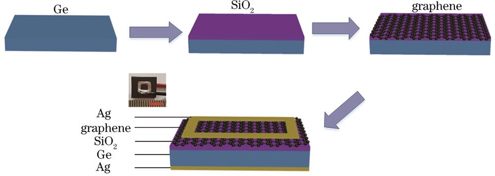
    Fig. 1. Fabrication process of the device
    Test principle of the device
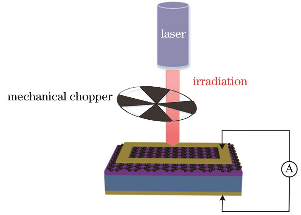
    Fig. 2. Test principle of the device
    Influence of dielectric layer thickness on device performance. (a) Dark current curve of the device; (b) spectral response curve of the device
    Fig. 3. Influence of dielectric layer thickness on device performance. (a) Dark current curve of the device; (b) spectral response curve of the device
    Raman spectra of graphene with different layers
    Fig. 4. Raman spectra of graphene with different layers
    Influence of the number of graphene layers on the device performance. (a) Spectral response of the graphene under zero bias; (b) dark current of the graphene
    Fig. 5. Influence of the number of graphene layers on the device performance. (a) Spectral response of the graphene under zero bias; (b) dark current of the graphene
    I-V curves of the device under different wavelengths of light
    Fig. 6. I-V curves of the device under different wavelengths of light
    Spectral response curves of Ge heterojunction and pure N-type Ge
    Fig. 7. Spectral response curves of Ge heterojunction and pure N-type Ge
    Responsivity of the device at different wavelengths
    Fig. 8. Responsivity of the device at different wavelengths
    Variation curves of device photocurrent and dark current with voltage
    Fig. 9. Variation curves of device photocurrent and dark current with voltage
    Responsiveness of the device under different bias voltages
    Fig. 10. Responsiveness of the device under different bias voltages
    Influence of excitation wavelength and bias voltage on device on/off ratio. (a) Influence of excitation wavelength on switching ratio; (b) influence of bias voltage on switching ratio
    Fig. 11. Influence of excitation wavelength and bias voltage on device on/off ratio. (a) Influence of excitation wavelength on switching ratio; (b) influence of bias voltage on switching ratio
    NPDR of the device at different wavelengths
    Fig. 12. NPDR of the device at different wavelengths
    Response time of the device
    Fig. 13. Response time of the device
    Band diagram of the device without oxide layer between graphene and Ge
    Fig. 14. Band diagram of the device without oxide layer between graphene and Ge
    Photoelectric response mechanism of the device. (a) Tunneling; (b) interface coupling
    Fig. 15. Photoelectric response mechanism of the device. (a) Tunneling; (b) interface coupling
    Device structureSpectral range /nmR /(A·W-1Ilight/IdarkResponse time /msRef.
    Gr-SiO2-Ge254-22000.0780.71×1041-3ours
    Gr-MoS25320.15×10-4//8
    Gr-Si5320.5110513×10-3-13.5×10-39
    Gr-Ge14000.0510423×10-3-108×10-31
    Gr-Al2O3-Ge520-16251.2104/10
    Table 1. Performance parameters of different devices
    Bei Li, Changlong Cai, Haifeng Liang, Feihu Fan, Ben Tu. Study on Broad Spectrum Photoelectric Properties of Graphene MIS Junction[J]. Laser & Optoelectronics Progress, 2022, 59(19): 1904001
    Download Citation