
Melissa Davis, Zhibin Yu. A review of flexible halide perovskite solar cells towards scalable manufacturing and environmental sustainability[J]. Journal of Semiconductors, 2020, 41(4): 041603
- Journal of Semiconductors
- Vol. 41, Issue 4, 041603 (2020)
Abstract
1. Introduction
Halide perovskites have quickly shown success as promising new photovoltaic materials. The record efficiency from such materials has reached 25.2% which rivals that of single junction silicon, the leading commercialized material[
Although perovskite solar cells have shown impressive efficiencies, they have accompanying challenges. Three of the most noted challenges for rigid PSCs are hysteresis, stability, and the use of lead. These disadvantages also affect flexible devices. To encourage commercialization, these factors need solutions. Therefore, for this review on flexible perovskite solar cells, additional focus will also be placed on these challenges. We will begin with an overview of the properties of the perovskite material followed by a section on hysteresis. The following section will address the instability seen in perovskite devices and proposed solutions. A focus on Ruddlesden-Popper perovskite solar cells will be discussed as a solution to the perovskite material’s instability. Commercialization is the focus of the final two sections where upscaling is discussed with a review on flexible PSCs and roll-to-roll PSCs. The final section relates to the environmental impact of PSCs where the focus is on lead and a cradle to grave assessment of the devices.
2. Basic properties of halide perovskites
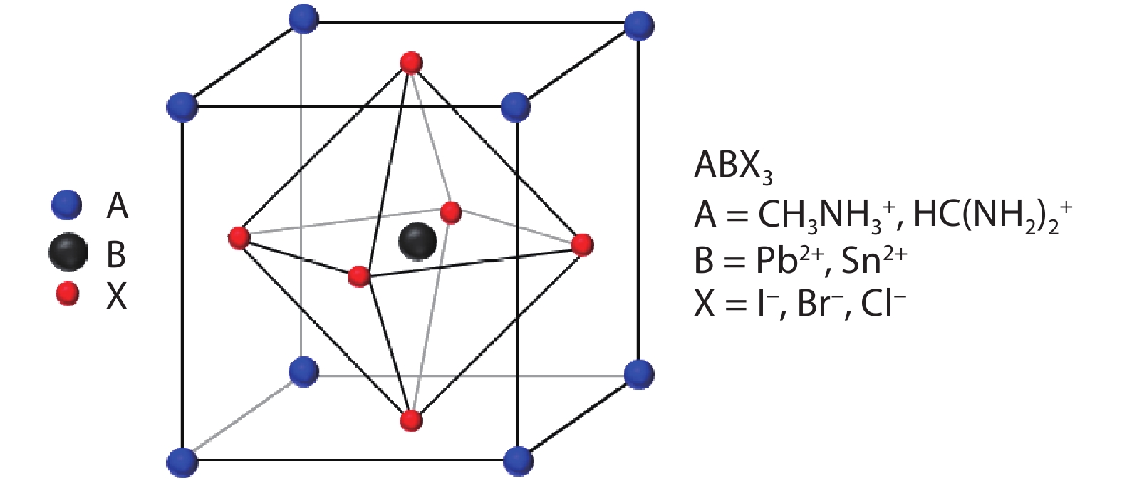
The perovskite material has many unique properties which promotes its ability to be an effective solar cell material. Perovskite solar cells utilize the perovskite crystalline structure. It can be found in nature; however, in solar cells, the crystal is synthesized in a laboratory setting. The general formula is ABX3 where ‘A’ and ‘B’ are cations and X is an anion. The perovskite crystal structure is cubic where ‘B’ is surrounded by an octahedron of X anions (Fig. 1)[
![]()
Figure 1.(Color online) Crystal structure diagram for the perovskite material[
Selection of ions has a direct impact on the geometric shape of the unit cell. The Goldschmidt tolerance factor, t, can be calculated to determine if the unit cell will remain cubic and stable. It is calculated through the ionic radii of each ion and is as follows:
where rA, rB, rX are the ionic radii of ‘A’, ‘B’, and ‘X’ ions. If the tolerance factor is less than one, the cubic structure will have distortion. The tolerance factor can be used to determine if selection of ions can create a formable perovskite structure[
Ion selection also has a direct impact on the bandgap of the material[
The perovskite material also has a superb absorption coefficient. An explanation for this property is its direct bandgap which minimizes loss of photon energy. Absorption coefficients are found by measuring light absorption of the material over a range of photon energies. MAPbI3 perovskites have a graph that is seen in Fig. 2. A sharp trend is seen at the bandgap near 1.5 eV; therefore, photons with energy at or above 1.5 eV have a high likelihood of being absorbed. A nearly perpendicular line shows that perovskite solar cells have a direct bandgap and structural order. Silicon SCs have a slower gradient on the rising edge; this corresponds with an indirect bandgap and more prevalent structural disorder[
![]()
Figure 2.(Color online) Absorption coefficients over photon energy for perovskite, GaAs, and single crystal silicon[
Another benefit of the perovskite material’s high absorption coefficient is ability to absorb photons with a thin layer. The coefficient varies over the range of photon energies and corresponding wavelengths. For MAPbI3 perovskite SCs, an absorption coefficient of 0.5 × 104 cm–1 at 700 nm was calculated[
3. Current challenges in perovskite solar cells
3.1. Hysteresis
Hysteresis is the phenomenon of differing efficiencies due to the scan direction of the testing equipment. A perovskite solar cell with hysteresis has two different results based on the scan direction and other factors. In addition, a PSC with hysteresis has different results due to previous tests; in other words, it has memory. Scan speed is another factor which affects hysteresis. Snaith et al. declares that fast scanning shows less hysteresis over slow scanning while other researchers formulate the inverse[
![]()
Figure 3.(Color online) Current–voltage performance of a PSC with (a) hysteresis properties and (b) no hysteresis properties. (c) Schematic diagram denoting potential causes of hysteresis in a PSC[
Two main causes for hysteresis have emerged: device materials and structure, and defects within the crystal. The former cause, device materials and structure, correlates to research which shows that the hysteresis effect is reduced in perovskite solar cells with an inverted structure[
The other main cause of hysteresis is believed to be due to defects within the crystalline structure[
While hysteresis is a problem in PSC, it can be minimized and removed through reducing defects and other trap states. It is still a continuing concern that plagues some PSCs; however, hysteresis is not a major concern for current record perovskite solar cells. Currently, the greatest issue plaguing perovskite solar cells is their short lifetime and instability.
3.2. Stability
Perovskite solar cells to demonstrate short lifetimes due to instability from various factors. The main challenge of perovskite solar cells is their stability. PSC cells have efficiencies which decrease over time due to degradation. This trend is not desired for commercialization and the decreasing efficiency is mainly caused by degradation of the perovskite layer. The four most common methods for perovskite film degradation is through moisture, oxygen, UV light, and heat. The perovskite material is sensitive to its environment during fabrication. Most perovskite layers are deposited and annealed within a controlled environment such as a nitrogen or argon filled glovebox. With a glovebox, the effect of the previously stated factors is significantly decreased.
The greatest threat to the perovskite structure, as well as the most studied, is moisture and humidity. Water is a strong enemy of perovskite films. Moisture easily breaks down the perovskite into its precursors[
![]()
Figure 4.(Color online) Time lapse of perovskite film degradation due to humidity[
One common method to combat the ingress of moisture is to increase the crystallinity of the perovskite structure. Noh et al. discovered that including a fraction of bromide into the perovskite structure shrinks the lattice to inhibit the entrance of water[
The second factor which most commonly affects perovskite films is oxygen. It is important to note that oxygen can only damage the film while the cell is illuminated[
![]()
Figure 5.(Color online) Stability depicted by change in absorption of perovskite films for two days in (a) illuminated, nitrogen atmosphere, (b) dark, nitrogen atmosphere, (c) illuminated, ambient atmosphere[
UV light can also degrade the film. PSCs with a layer of TiO2 are especially vulnerable to degradation due to UV light[
![]()
Figure 6.(Color online) Effect of UV light stability due to percentage of bromide included in PSC[
The final degradation method is thermal irradiation or heat. High temperatures can cause the perovskite structure to change its phase. With regards to heat degradation, the ‘A’ ion has the greatest effect on thermal stability. The common PSC utilizes MAI which is more reactive than other ‘A’ ions such as Cs or FAI[
Stability is a major concern for the commercialization prospects of PSCs. The two leading sources of instability are moisture and oxygen. Perovskite degradation is greatly fueled by the generation of water within the perovskite which quickly breaks down the two components of the structure. Methods to reduce this occurrence focus on creating a stronger crystalline lattice with compositional changes. A solution to the threat of degradation can be through encapsulation and the use of Ruddlesden-Popper perovskites.
3.2.1. Encapsulation
A method to reduce the hazard of lead and improve stability of PSC is through encapsulation. It is also a completely necessary step for commercialization. The most common methods to encapsulate solution processed solar cells is with a glass cover and epoxy. Encapsulation is key to protect the perovskite film from outer elements, as well as to protect the environment from chemical elements which may be detrimental to nature.
The cell can be encapsulated by sandwiching the glass substrate with the layers between another flat glass slide and filling remaining space with an epoxy resin. Another option is to use a ‘U’ shaped glass cover with an internal desiccant. In this set-up, the epoxy resin is only used on the outer edges to create a complete seal between the bottom glass substrate and the upper glass cover[
![]()
Figure 7.(Color online) Encapsulation methods for PSCs (a) with a full covering of epoxy and (b) with a ‘u’-shaped glass cover and a desiccant[
3.2.2. Ruddlesden-Popper perovskite solar cells
Another method to improve perovskite solar cell’s stability is the introduction of two-dimensional perovskite structures. Two-dimensional perovskite structures for solar cells are commonly large organic cations which grow in flat sheets. By nature, they are hydrophobic and slightly insulating[
![]()
Figure 8.(Color online) Three common examples of 2D perovskites as the active layer of PSCs[
The ratio of 2D perovskite to 3D perovskite is key for the distinction between groups. If there is a small amount of 2D within the 3D perovskite, a mixed or passivated layer will be created. If there is a more similar ratio, such a one-part 2D perovskite to five parts 3D perovskite, then a periodic pattern will emerge. See Fig. 9 for a graphical description of some of the 2D material structure options.
![]()
Figure 9.(Color online) Crystal Structures of Ruddlesden-Popper and Dion-Jacobson perovskites[
The Ruddlesden-Popper perovskite structure is one type of the periodic patterns which can emerge. It is the most common and is seen when the 2D layers slice the 3D matrix within the [110] direction. Another type of perovskite structure is the Dion-Jacobson or DJ type. A main difference between the two is that DJ type perovskites are suited to wide-infrared range[
The Ruddlesden-Popper perovskite structure utilizes a layer structure with 2D and 3D structures intermixed in a periodic pattern. The distance between the 2D material is typically denoted by an ‘n’. If the ‘n’ is one, then there is one layer of 3D perovskite between each 2D layer. If the ‘n’ is five, there are five rows of the 3D perovskite between each 2D layer. A pure 3D perovskite solar cell has an ‘n’ of infinity; it has indefinite layers of the 3D perovskite with no 2D perovskite layers[
![]()
Figure 10.(Color online) Crystal structure for Ruddlesden-Popper perovskites with increasing ‘
In addition to 2D perovskite’s hydrophobic nature, the layered structure creates natural quantum wells which lead to more insulating behaviors[
Material selection is key for Ruddlesden-Popper solar cells much like pure 3D perovskite solar cells. The general chemical structure for RPSCs is
Processing of Ruddlesden-Popper perovskites
An issue with Ruddlesden-Popper, or RP, cells is that their periodic nature is not guaranteed to be consistent throughout the layer. While stoichiometry can control the ‘n’ layers, layers of differing ‘n’ values grow. Research has found that controlling the ‘n’ layers to values between one and five allows for higher success in creating phase pure films[
Growth orientation is a key research focus. The crystallinity can grow parallel, perpendicular, or nonuniformly to the substrate (Fig. 11)[
![]()
Figure 11.(Color online) Growth orientations of Ruddlesden-Popper perovskites: horizontal and vertical[
Various processes have been discovered to change the growth orientation. One such way is utilizing a process called hot pressing or hot casting. Hot casting is when the substrate is preheated before the layer is applied with spin-coating. Most researchers heat their substrate to temperatures around 150 °C and then quickly move it to the spin coater. Another method to grow crystals out of plane is through the manipulation of solvents[
![]()
Figure 12.(Color online) Solvent effect on growth direction for pure DMF, equal parts DMF and DMSO, and pure DMSO[
Another method to control growth orientation is through selection of spacing cations. There are nearly limitless options for 2D perovskite cations. The main benefits of utilizing a 2D cation is its ability to improve crystallinity and increase stability. Selection of cations is an optimization of the benefits. In addition, size or length of cations is useful. The length of the 2D spacer cations is directly related to the bandgap. Compounds with a longer chain length lead to films with higher bandgaps due to the insulating properties of long chains[
Ruddlesden-Popper devices with PEA
In 2014, Smith et al. published work on one of the first Ruddlesden-Popper PSCs. The 2D material was phenethyl ammonium or PEA and an efficiency of 4.73% was discovered[
Further improvement of PEA was published in 2019 by Shi et al.[
Ruddlesden-Popper devices with BA
The most commonly used A’ compound is CH3(CH2)3NH3 or n-butylammonium. It is also typically shortened into BA or n-BA[
![]()
Figure 13.(Color online) Normalized efficiency of BA RPPSCs over time with (a) constant illumination while unencapsulated, (b) unencapsulated in humidity, (c) constant illumination while encapsulated, and (d) encapsulated in humidity[
Work was continued in the following years to further improve the efficiency of BA RPPSCs. Researchers have focused on those with a ‘n’ value of four. In 2017, Zhang et al. shared their success in creating a BA PSC with an efficiency of 13.7%[
Research has focused upon RPPSCs with an ‘n’ value of four due to BA’s nature to create films with perpendicular orientation at that ‘n’ value. In addition, the Urbach energy of each increasing ‘n’ level until four was discovered to confirm higher structural order and a direct bandgap. Urbach energy for RPPSCs with BA have an energy of 37, 20, and 18 meV for ‘n’ values from two to four. While the pure 3D Urbach energy is 16 meV, which is smaller, inclusion of BA drastically improves the stability[
Alternative materials for Ruddlesden-Popper devices
One downfall of utilizing BA as a spacing ion is its longer length which causes a larger bandgap and therefore lower efficiency. In response to this issue, alternative materials have been discovered. BYA or 3-butyn-1-amine and BEA or 1-amino-2-butene 2D perovskites were used to replace BA. In the ‘n’ of four set-up, higher efficiencies were discovered due to BYA and BEA’s ability to reduce the active layer’s roughness and increase crystallinity due to their decreased length[
The current leading efficiency for Ruddlesden-Popper PSCs is 18.2% with the work of Yang et al. in 2018. The 2D cation used was 3-bromobenzylammonium iodide or 3BBAI[
Stability is one of the key problems that plague the perovskite material. Addition of 2D perovskites to form Ruddlesden-Popper films is a key solution to this problem. Inclusion of the hydrophobic 2D perovskites allows for cells to be manufactured in open air unlike the nitrogen filled gloveboxes that pure 3D devices require. The tolerance to oxygen and moisture allowed for further development of tin perovskite devices. Selection of the 2D ion is an important research area. PEA and BA first emerged as the leading 2D perovskites. Further optimization discovered the current record RPPSC device with 3BBAI and an efficiency of 18.2%. Solution processing and hot casting were used to make the film.
Perovskite solar cells face a few issues such as hysteresis and stability. With crystallinity optimization processes, hysteresis has significantly decreased. More stable devices have been achieved with the inclusion of Ruddlesden-Popper perovskites.
An important factor for commercialization is the lifetime and stability of the devices. Energy payback time, or EPBT, is an important measure for renewable energy technologies. It is also another advantage of PSCs. Since photovoltaics require a high upfront cost, EPBT is calculated to determine how quickly consumers will recuperate their cost and begin profiting from their investment. Silicon SCs have an EPBT of about 2–3 years while perovskite SCs have an EPBT of 0.25–0.3 years, or 3–4 months[
![]()
Figure 14.(Color online) Energy payback times per photovoltaic material where P-1 and P-2 are two PSCs with different layers[
Perovskite’s short EPBT is very beneficial when paired with its stability concerns. With a shorter payback time, shorter lifetimes are acceptable. Gong et al. place a conservative estimate that current PSC technology will grant devices with 2–3 years of stability[
4. Flexible perovskite solar cells
One of the main reasons for the perovskite structure’s success is due to its unique crystalline properties. The perovskite structure self-crystallizes with minimal defects which allow for superb electronic properties. Its ability to be solution processed is a major advantage when looking to commercialize the technology. Flexible perovskite solar cells hold specific advantages over its rigid counterparts. These devices have applications in many new fields such as wearable electronics, curved electronic displays, and portable electronics[
An additional advantage of flexible devices is their reduced cost. The highest cost layer of a perovskite solar cell is the ITO glass substrate[
R2R is the method that commonly makes newspapers. The substrate begins blank on a beginning roll. It is then unraveled and pulled through various printing processes and raveled back onto a final roll. For PSCs using R2R processing, the intermediate steps are the most important as they add the layers. There are multiple printing processes which can be used to add layers.Fig. 15 depicts the production of fPSCs with R2R processing for all layers.
![]()
Figure 15.(Color online) (a) Sequential processing of R2R production for all steps. (b) Slot die printing apparatus. (c) Resulting fPSC device. (d) Razza
There are additional printing methods for upscaling the manufacturing of perovskite films such as screen printing and ink-jet printing. Screen printing is the process where ink is transferred onto surfaces after being spread across a mesh screen which acts as a blocking stencil. For perovskite solar cells, the hole and electron transport layers are screen printed onto the substrates[
Roll to roll processing requires the use of flexible perovskite solar cells. Perovskite films have demonstrated success tolerating stress and strain during flexing. The perovskite material’s flexible properties are postulated to be due to small grains within the crystalline structure. Liu et al. believes that larger grains would break into smaller grains during flexing thus causing more grain boundaries and separation between the perovskite and surrounding layers[
To better understand flexible PSCs, or fPSCs, a review of the material selection and properties is necessary.
4.1. Substrate materials
The substrate is arguably the most important layer in flexible PSCs. It is the backbone to the fPSC which allows the cells to flex, while also protecting and encapsulating the materials within. There are two main types of substrates that can be used: polymer films and thin metal films[
Flexible thin metal foils are favorable materials for fPSCs due to their strong mechanical properties and tolerance to high temperatures. Their greatest disadvantage is their opaque nature, which requires their placement in the back of the cell structure. The most commonly used thin metal film is titanium foil[
Titanium foil is frequently used because a common layer within record, rigid PSCs is TiO2. TiO2 requires high annealing temperatures which metal foils can tolerate. In addition, oxidation of titanium foil can create a layer of TiO2. The layers of the device are deposited sequentially and the outer most layer must be transparent. To complete the cell, a transparent, outer electrode is required. Researchers have used glass and a polymer laminate to complete the cell; glass is irrelevant for fPSC applications.
The record device utilizing a titanium foil substrate was made in 2018 by Han et al.[
![]()
Figure 16.(Color online) fPSC device structure of Han
The greatest disadvantage to metal films is their lack of transparency. This requires the structure to be reversed which inhibits its growth as a fPSC substrate. Polymer substrates are much more commonly used.
PET films, or polyethylene terephthalate, are one of the commonly utilized polymer substrates. It has a high transparency, flexibility, and resistance to solvents. PET’s greatest downfall is its low melting temperature. It cannot tolerate temperatures near 200 °C without melting, with a maximum working temperature of 120 °C[
Another similar polymer substrate is PEN, or polyethylene naphtalate. PEN shares PET’s properties such as transparency and flexibility. PEN has a slightly higher tolerance to heat with a maximum working temperature at 155 °C. The greatest downfall of PET and PEN is their high water-vapor-transmission-rate, or WVTR. The WVTR of PET was calculated to be about 1.1 g/(m2·day) at 45 °C for a film with thickness 100 µm[
Despite these disadvantages, most of the reported fPSCs utilize either PEN or PET as their substrate. In 2019, Zhu et al. demonstrated fPSCs on PET with an efficiency of 18.53%[
The disadvantages of PEN and PET, such as their high WVTR and oxygen infiltration, have led researchers to search for replacement materials. One such material is CPI or colorless polyimide[
Another substrate option is flexible glass, or willow glass. Willow glass can tolerate temperatures up to 700 °C while allowing for high transparency and an excellent WVTR[
4.2. Transparent conductive electrodes
For rigid PSCs, the most commonly used material for the front electrode is either indium tin oxide, ITO, or fluorine-doped tin oxide, FTO, glass. The most used transparent conductive electrode, or TCO, for fPSCs is ITO. While FPSCs commonly use ITO as their transparent electrode, research has shown that ITO is a brittle layer which commonly cracks and leads to FPSC’s failure[
One method to mitigate ITO’s tendency to crack was shown with the use of a sandwiched device structure where PEN with ITO is on both sides of the perovskite film. With this structure and by placing the perovskite and additional layers within the center or neutral position in the cell, the cracks were significantly minimized[
![]()
Figure 17.(Color online) (a) Schematic view of PEN sandwich set-up for (a1) single PEN, (a2) double PEN with 125
ITO’s brittle effects have also shown to be minimized with the use a new substrate, colorless polyimide or CPI. Through 10 000 cycles of bending fatigue tests, the ITO showed little to no cracking as seen with the surface SEM images (Fig. 18)[
![]()
Figure 18.SEM Images of (a) ITO on PET with ITO flexed outward and inward, (b) ITO on CPI with ITO flexed outward and inward[
Aluminum zinc oxide, or AZO, and indium zinc oxide, or IZO, have been used as a replacement for ITO. The performance of the three were compared on willow glass by Dou et al. in 2017[
Another replacement TCO material used is a silver nanowire mesh. While silver nanowires have excellent flexibility and low resistivity, silver can break down the perovskite layer. When used as an electrode previously, silver diffuses into the perovskite active layer and creates a silver halide[
Graphene is another replacement material. Graphene has an improved ability to flex without cracking. A thin layer of graphene is used as the TCO and can be applied through chemical vapor deposition, or CVD or spin coating. In 2017, Yoon et al. used CVD to apply graphene onto its substrate of PEN. Their research demonstrated a hysteresis-free fPSC with an efficiency of 16.8%; their device showed a tolerance to 5000 bends of radius 2 mm while maintaining 85% of its efficiency[
4.3. Manufacturing of record fPSCs
The fPSC with record efficiencies use the conventional planar structure. In June 2019, Wu et al. demonstrated a fPSC on PEN with an efficiency of 19.38%[
![]()
Figure 19.(Color online) Perovskite film deposition method by Wu
Flexible PSCs with an inverted planar structure are also seen; however, their efficiency is less than fPSCs with a conventional structure. The current record efficiency for fPSCs with an inverted planar structure is 18.1%[
![]()
Figure 20.Device structure of inverted fPSC with an efficiency of 18.1% ITO/PET/perovskite/fullerene/BCP/Copper[
One of the main issues with current record flexible PSCs is that their production methods are not fully compatible with R2R processing. Spin coating is a commonly used deposition method and the back electrode is typically thermally evaporated. Four of the most common printing methods for R2R processing are spray coating, slot-die coating, blade coating, and inkjet printing. The general description for each method has been described previously. The printing method most paired with R2R printing for fPSCs is a slot-die method.
Schmidt et al. demonstrated one of the first examples of a fully R2R printed fPSC in 2015[
Hwang et al. later demonstrated R2R printing of fPSCs with an efficiency of 11.94% in 2015[
![]()
Figure 21.(Color online) (a1) Cell structure with energy band levels. (a2) Slot die set-up with gas quenching attachment. (b) Roll to Roll manufacturing set-up seen in stages (b1) PbI2 deposited (b2) PbI2 layer annealed with gas quenching (b3) resulting film after MAI[
Further research was done to simplify the steps of deposition while better understanding how to create highly crystalline films with slot-die deposition. Zuo et al. demonstrated a one-step method to create fPSCs with R2R methods; their work showed an efficiency of 11.16%[
![]()
Figure 22.(Color online) (a) Perovskite deposition method by Zuo
Researchers from the Netherlands developed a method to create fPSCs with R2R processing with a record high efficiency of 13.5%[
Galagan et al. made an important note and declared that their efficiency could be higher at 14.5% if the area of the devices were decreased to 0.04 cm2, the typical area of record PSC[
A remarkable discovery found while researching flexible PSCs is that the perovskite material tends to not be the limiting factor. In other words, other layers such as the TCO are the main reason for degradation during flexing, not the perovskite layer. Various flexible substrates were studied. The substrates’ heat instability is their greatest downfall. Therefore, fPSCs deposit their layers with lower temperatures. Devices with high efficiencies were still shown for fPSCs with a record efficiency of 19.38%.
The success of fPSCs lead to the advancement of R2R processes for perovskite solar cells. R2R processes allow for reduced manufacturing time and cost for fPSCs. Efficiencies as high as 13.5% were reported with R2R methods; however, devices with higher efficiencies do not use R2R methods for all their steps.
To ensure for success in commercialization the sustainability of producing the materials is important. Record devices use lead. While solar energy is known to produce electricity with minimal environmental impact, an analysis on its production and materials is necessary.
5. Sustainability of perovskite solar cells
There are two main sections of sustainability for perovskite solar cells. The primary concern for perovskite solar cells is their use of lead. It is also important that the impact of complete perovskite solar cell devices from cradle to grave is completed to ensure environmental risks and impacts are minimized.
5.1. Impact of lead
A major disadvantage and concern for using PSCs is their use of lead. Perovskite solar cells with the highest efficiency utilize lead as one of their ions. Due to lead’s toxicity, its use is discouraged. Another disadvantage of lead in PSC is its increased solubility in water[
A natural replacement for lead is tin. In 2014, Hao et al. demonstrated the first PSC lead-free device with an efficiency of 5.73%[
Another option to replace lead is with a double perovskite structure. In this structure two divalent ions, typically Pb2+, are replaced with one monovalent and one trivalent ion[
Lead-free PSC are desirable to reduce environmental harm; however, the risk of using lead can be mitigated through encapsulation and careful processing procedures. A key fact which helps further mitigate this problem is that the lead in perovskite solar cells is equal to the amount of lead in soil of the same area with 1 cm depth[
Lead is most found in lead-acid batteries for cars. The lead is contained in the leads of both sides of the battery and is a component of the internal structure as well[
![]()
Figure 23.(Color online) Conversion of 1 lead-acid battery into 709 m2 PSCs and power for 30.2 homes in Las Vegas[
The same researchers determined that utilizing the lead from lead-acid batteries is also more environmentally friendly than extraction from lead ore (Fig. 24). With their lead extraction process, lower temperatures are utilized, and harmful emissions are avoided[
![]()
Figure 24.(Color online) Refining processes for PbI2 in perovskite solar cells when harvest from raw lead ore or car batteries[
Recycling of the lead within spent perovskite solar cells has also been shown. In order to remove and reuse the lead within the PSC, the layers above the perovskite must be removed. The layers can be removed sequentially or all at once. The outermost metal layer, commonly gold or aluminum, can be removed with scotch tape or by delaminating it from the layer beneath. The metal can be extracted through filtration of the solution. Although lead is the focus, recycling the metal electrode is very useful as it is one of the most expensive layers[
Complete removal of the layers together is another method that has been researched. Kim et al. used a polar aprotic solvent such as DMF, GBL, or DMSO to dissolve the all the layers except the TiO2[
![]()
Figure 25.(Color online) Two-step process of Kim
Reports of lead recycling are few, with the focus on rigid perovskite solar cells. Although research has not been extensively done on flexible PSCs, similar methods are applicable. The main concern of using flexible substrates is the possible breakdown that can occur when polymer substrates are subjected to certain solvents. Fortunately, the two most commonly used polymer substrates, PEN & PET, are resistant to most chemical degradation. Solvents such as trifluoro acetic acid can dissolve PET but solvents such as DMSO, DMF, and GBL are viewed as insoluble for PET [
In conclusion, lead within perovskite solar cells is toxic; however, the amount used per device is minimal when compared to the lead required for vehicle batteries. Replacement of lead with tin has been suggested. Unfortunately, tin iodide has been shown to be more toxic than lead ioidide. Therefore, with proper recycling programs, the risk of lead can be minimized. In addition, spent lead-acid batteries from cars can be redirected to be reused in PSCs.
5.2. Impact of complete perovskite devices
A cradle to grave analysis of perovskite devices is key to ensure the renewable technology minimizes environmental impact. An in-depth review of 16 environmental risk factors was completed for perovskite solar cell devices by Gong et al. They compared the impact of two conventional structure PSCs. The first of which was FTO/ TiO2/perovskite/spiro-OMeTAD/Au and the second structure was ITO/ZnO/perovskite/Ag[
![]()
Figure 26.(Color online) Environmental Profile of FTO/TiO2/perovskite/spiro/Au focus should be given to the factors highlighted with a red box[
![]()
Figure 27.(Color online) Environmental profile of ITO/ZnO/perovskite/Ag[
Another factor calculated was Eco-indicator 99; this factor indicators the environmental impact of a product in three damage categories: human health, ecosystem quality, and resources[
![]()
Figure 28.(Color online) Holistic impact of various PV materials on resources, human health, and ecosystem quality P-1 is FTO/ TiO2/perovskite/spiro/Au P-2 is ITO/ZnO/perovskite/Ag[
Gold is a highly impactful element used in PSCs; it requires extensive land use to mine and processing of it releases harmful by-products[
A final environmentally impactful element of PSC production is the use of solvents. Solvents pose the greatest direct threat to processing as their risks are assumed during this step. Commonly used solvents are DMF, NMP, DMSO, and GBL[
An interesting note is the lack of lead’s toxicity in the environmental impact of both perovskite architectures. Despite the fact that lead in PSCs is soluble in water, its impact is limited due to its small amount used.
While replacement mitigates many safety concerns, risk will still remain during processing. Currently, these risks are managed in a laboratory setting with a glovebox and fume hood. These devices protect users from inhalation of solvents with enclosed set-ups and decreased vapor pressure. With the scaling up required of commercialization, similar precautions can be taken. Moderate encapsulation with negative pressure will alleviate the risk of solvents. The encapsulation of the processing line will be required anyway to reduce contaminants.
6. Conclusion
Perovskite solar cells have demonstrated great promise as a new solar energy technology. Their excellent properties and solution processing ability make them a solid contender as the next commercialized photovoltaic material. While the material struggles with instability, methods to counteract degradation have been developed with the use of Ruddlesden-Popper perovskites. Once stabilized, commercialization requires an upscaling of manufacturing. The perovskite material also demonstrates a tolerance to flexing which has allowed for its success as a flexible device. When combined with roll-to-roll processing, commercialization of this technology progresses forward. A final consideration of the environmental impact of perovskite devices is necessary. Despite the concern of many researchers to remove lead, devices use minimal amounts and it can be possibly recycled. A cradle to grave assessment of the technology determined that the use of solvents, gold, and ITO glass impacts the environment more substantially. Methods to reduce such risks are suggested.
Acknowledgements
The authors are thankful to the financial support by National Science Foundation under Award ECCS-1609032.
References
[1]
[2] N G Park. Perovskite solar cells: an emerging photovoltaic technology. Mater Today, 18, 65(2015).
[3] R Wang, M Mujahid, Y Duan et al. A review of perovskites solar cell stability. Adv Funct Mater, 0, 1808843(2019).
[4]
[5] C Li, X Lu, W Ding et al. Formability of ABX3 (X = F, Cl, Br, I) halide perovskites. Acta Crystallogr B, 64, 702(2008).
[6] I E Castelli, J M García-Lastra, K S Thygesen et al. Bandgap calculations and trends of organometal halide perovskites. APL Mater, 2, 081514(2014).
[7] L Wang, G D Yuan, R F Duan et al. Tunable bandgap in hybrid perovskite CH3NH3Pb(Br3–
[8] S De Wolf, J Holovsky, S J Moon et al. Organometallic halide perovskites: sharp optical absorption edge and its relation to photovoltaic performance. J Phys Chem Lett, 5, 1035(2014).
[9] M Ledinsky, T Schönfeldová, J Holovský et al. Temperature dependence of the urbach energy in lead iodide perovskites. J Phys Chem Lett, 10, 1368(2019).
[10] G Xing, N Mathews, S Sun et al. Long-range balanced electron- and hole-transport lengths in organic-inorganic CH3NH3PbI3. Science, 342, 344(2013).
[11] S D Stranks, G E Eperon, G Grancini et al. Electron-hole diffusion lengths exceeding 1 micrometer in an organometal trihalide perovskite absorber. Science, 342, 341(2013).
[12] J Peng, Y Chen, K Zheng et al. Insights into charge carrier dynamics in organo-metal halide perovskites: from neat films to solar cells. Chem Soc Rev, 46, 5714(2017).
[13] H J Snaith, A Abate, J M Ball et al. Anomalous hysteresis in perovskite solar cells. J Phys Chem Lett, 5, 1511(2014).
[14] Y Shao, Z Xiao, C Bi et al. Origin and elimination of photocurrent hysteresis by fullerene passivation in CH3NH3PbI3 planar heterojunction solar cells. Nat Commun, 5, 5784(2014).
[15] N K Elumalai, M A Mahmud, D Wang et al. Perovskite solar cells: progress and advancements. Energies, 9, 861(2016).
[16] D H Kang, N G Park. On the current–voltage hysteresis in perovskite solar cells: dependence on perovskite composition and methods to remove hysteresis. Adv Mater, 0, 1805214(2019).
[17] H S Kim, I H Jang, N Ahn et al. Control of
[18] A Fakharuddin, U Shabbir, W Qiu et al. Inorganic and layered perovskites for optoelectronic devices. Adv Mater, 0, 1807095(2019).
[19] D Y Son, S G Kim, J Y Seo et al. Universal approach toward hysteresis-free perovskite solar cell via defect engineering. J Am Chem Soc, 140, 1358(2018).
[20] Y Rong, Y Hu, A Mei et al. Challenges for commercializing perovskite solar cells. Science, 361, eaat8235(2018).
[21] C C Boyd, R Cheacharoen, T Leijtens et al. Understanding degradation mechanisms and improving stability of perovskite photovoltaics. Chem Rev, 119, 3418(2019).
[22] C Ma, C Leng, Y Ji et al. 2D/3D perovskite hybrids as moisture-tolerant and efficient light absorbers for solar cells. Nanoscale, 8, 18309(2016).
[23] J H Noh, S H Im, J H Heo et al. Chemical management for colorful, efficient, and stable inorganic–organic hybrid nanostructured solar cells. Nano Lett, 13, 1764(2013).
[24] Q Tai, P You, H Sang et al. Efficient and stable perovskite solar cells prepared in ambient air irrespective of the humidity. Nat Commun, 7, 11105(2016).
[25] Q Jiang, D Rebollar, J Gong et al. Pseudohalide-induced moisture tolerance in perovskite CH3NH3Pb(SCN)2I thin films. Angew Chem, 127, 7727(2015).
[26] K Domanski, E A Alharbi, A Hagfeldt et al. Systematic investigation of the impact of operation conditions on the degradation behaviour of perovskite solar cells. Nat Energy, 3, 61(2018).
[27] D Bryant, N Aristidou, S Pont et al. Light and oxygen induced degradation limits the operational stability of methylammonium lead triiodide perovskite solar cells. Energy Environ Sci, 9, 1655(2016).
[28] G Y Kim, A Senocrate, T Y Yang et al. Large tunable photoeffect on ion conduction in halide perovskites and implications for photodecomposition. Nat Mater, 17, 445(2018).
[29] M I Saidaminov, J Kim, A Jain et al. Suppression of atomic vacancies via incorporation of isovalent small ions to increase the stability of halide perovskite solar cells in ambient air. Nat Energy, 3, 648(2018).
[30] S D Stranks, H J Snaith. Metal-halide perovskites for photovoltaic and light-emitting devices. Nat Nanotechnol, 10, 391(2015).
[31] M Ouafi, B Jaber, L Atourki et al. Improving UV stability of MAPbI3 perovskite thin films by bromide incorporation. J Alloys Compd, 746, 391(2018).
[32] F Li, M Liu. Recent efficient strategies for improving the moisture stability of perovskite solar cells. J Mater Chem, A, 5, 15447(2017).
[33] Y Han, S Meyer, Y Dkhissi et al. Degradation observations of encapsulated planar CH3NH3PbI3 perovskite solar cells at high temperatures and humidity. J Mater Chem, A, 3, 8139(2015).
[34] D H Cao, C C Stoumpos, T Yokoyama et al. Thin films and solar cells based on semiconducting two-dimensional Ruddlesden–Popper (CH3(CH2)3NH3)2(CH3NH3)
[35] P Chen, Y Bai, S Wang et al. In situ growth of 2D perovskite capping layer for stable and efficient perovskite solar cells. Adv Funct Mater, 28, 1706923(2018).
[36] L Gao, F Zhang, C Xiao et al. Improving charge transport via intermediate-controlled crystal growth in 2D perovskite solar cells. Adv Funct Mater, 0, 1901652(2019).
[37] D H Cao, C C Stoumpos, O K Farha et al. 2D homologous perovskites as light-absorbing materials for solar cell applications. J Am Chem Soc, 137, 7843(2015).
[38] C Ortiz-Cervantes, P Carmona-Monroy, D Solis-Ibarra. Two-dimensional halide perovskites in solar cells: 2D or not 2D. ChemSusChem, 12, 1560(2019).
[39] I C Smith, E T Hoke, D Solis-Ibarra et al. A layered hybrid perovskite solar-cell absorber with enhanced moisture stability. Angew Chem, 126, 11414(2014).
[40] H Hu, T Salim, B Chen et al. Molecularly engineered organic-inorganic hybrid perovskite with multiple quantum well structure for multicolored light-emitting diodes. Sci Rep, 6, 33546(2016).
[41] C C Stoumpos, C M M Soe, H Tsai et al. High members of the 2D Ruddlesden-Popper halide perovskites: synthesis, optical properties, and solar cells of (CH3(CH2)3NH3)2(CH3NH3)4Pb5I16. Chem, 2, 427(2017).
[42] W Shockley, H J Queisser. Detailed balance limit of efficiency of p-n junction solar cells. J Appl Phys, 32, 510(1961).
[43] J C Blancon, H Tsai, W Nie et al. Extremely efficient internal exciton dissociation through edge states in layered 2D perovskites. Science, eaal4211(2017).
[44] L Chao, T Niu, Y Xia et al. Efficient and stable low-dimensional Ruddlesden–Popper perovskite solar cells enabled by reducing tunnel barrier. J Phys Chem Lett, 10, 1173(2019).
[45] Y Chen, Y Sun, J Peng et al. 2D Ruddlesden–Popper perovskites for optoelectronics. Adv Mater, 30, 1703487(2018).
[46] J Yan, W Qiu, G Wu et al. Recent progress in 2D/quasi-2D layered metal halide perovskites for solar cells. J Mater Chem A, 6, 11063(2018).
[47] H Li, X Wang, T Zhang et al. Layered Ruddlesden–Popper efficient perovskite solar cells with controlled quantum and dielectric confinement introduced via doping. Adv Funct Mater, 29, 1903293(2019).
[48] J Shi, Y Gao, X Gao et al. Fluorinated low-dimensional Ruddlesden–Popper perovskite solar cells with over 17% power conversion efficiency and improved stability. Adv Mater, 31, 1901673(2019).
[49] H Tsai, W Nie, J C Blancon et al. High-efficiency two-dimensional Ruddlesden–Popper perovskite solar cells. Nature, 536, 312(2016).
[50] X Zhang, X Ren, B Liu et al. Stable high efficiency two-dimensional perovskite solar cells via cesium doping. Energy Environ Sci, 10, 2095(2017).
[51] S Zhang, S M Hosseini, R Gunder et al. The role of bulk and interface recombination in high-efficiency low-dimensional perovskite solar cells. Adv Mater, 31, 1901090(2019).
[52] R Yang, R Li, Y Cao et al. Oriented quasi-2D perovskites for high performance optoelectronic devices. Adv Mater, 30, 1804771(2018).
[53] M M Lunardi, A W Y Ho-Baillie, J P Alvarez-Gaitan et al. A life cycle assessment of perovskite/silicon tandem solar cells. Prog Photovolt Res Appl, 25, 679(2017).
[54] J Gong, S B Darling, F You. Perovskite photovoltaics: life-cycle assessment of energy and environmental impacts. Energy Environ Sci, 8, 1953(2015).
[55] H Dong, J Xi, L Zuo et al. Conjugated molecules “bridge”: functional ligand toward highly efficient and long-term stable perovskite solar cell. Adv Funct Mater, 29, 1808119(2019).
[56] D Yang, R Yang, S Priya et al. Recent advances in flexible perovskite solar cells: fabrication and applications. Angew Chem Int Ed, 58, 4466(2019).
[57] J Y Lam, J Y Chen, P C Tsai et al. A stable, efficient textile-based flexible perovskite solar cell with improved washable and deployable capabilities for wearable device applications. RSC Adv, 7, 54361(2017).
[58] A Binek, M L Petrus, N Huber et al. Recycling perovskite solar cells to avoid lead waste. ACS Appl Mater Interfaces, 8, 12881(2016).
[59] S Razza, S Castro-Hermosa, A Di Carlo et al. Research update: large-area deposition, coating, printing, and processing techniques for the upscaling of perovskite solar cell technology. APL Mater, 4(2016).
[60] A Bashir, S Shukla, Lew Haur et al. Spinel Co3O4 nanomaterials for efficient and stable large area carbon-based printed perovskite solar cells. Nanoscale, 10, 2341(2018).
[61] K Cao, Z Zuo, J Cui et al. Efficient screen printed perovskite solar cells based on mesoscopic TiO2/Al2O3/NiO/carbon architecture. Nano Energy, 17, 171(2015).
[62] P Li, C Liang, B Bao et al. Inkjet manipulated homogeneous large size perovskite grains for efficient and large-area perovskite solar cells. Nano Energy, 46, 203(2018).
[63] Z Wei, H Chen, K Yan et al. Inkjet printing and instant chemical transformation of a CH3NH3PbI3/nanocarbon electrode and interface for planar perovskite solar cells. Angew Chem Int Ed, 53, 13239(2014).
[64] X Liu, X Guo, Y Lv et al. Enhanced performance and flexibility of perovskite solar cells based on microstructured multilayer transparent electrodes. ACS Appl Mater Interfaces, 10, 18141(2018).
[65] V Zardetto, T M Brown, A Reale et al. Substrates for flexible electronics: a practical investigation on the electrical, film flexibility, optical, temperature, and solvent resistance properties. J Polym Sci B, 49, 638(2011).
[66] H Xie, X Yin, Y Guo et al. Recent progress of flexible perovskite solar cells. Phys Status Solidi RRL, 13, 1800566(2019).
[67] G S Han, S Lee, M L Duff et al. Highly bendable flexible perovskite solar cells on a nanoscale surface oxide layer of titanium metal plates. ACS Appl Mater Interfaces, 10, 4697(2018).
[68]
[69] N Zhu, X Qi, Y Zhang et al. High efficiency (18.53%) of flexible perovskite solar cells via the insertion of potassium chloride between SnO2 and CH3NH3PbI3 layers. ACS Appl. Energy Mater, 2, 3676(2019).
[70] C Wu, D Wang, Y Zhang et al. FAPbI3 flexible solar cells with a record efficiency of 19.38% fabricated in air via ligand and additive synergetic process. Adv Funct Mater, 29, 1902974(2019).
[71] J I Park, J H Heo, S H Park et al. Highly flexible InSnO electrodes on thin colourless polyimide substrate for high-performance flexible CH3NH3PbI3 perovskite solar cells. J Power Sources, 341, 340(2017).
[72] M M Tavakoli, K H Tsui, Q Zhang et al. Highly efficient flexible perovskite solar cells with antireflection and self-cleaning nanostructures. ACS Nano, 9, 10287(2015).
[73] B Dou, E M Miller, J A Christians et al. High-performance flexible perovskite solar cells on ultrathin glass: implications of the TCO. J Phys Chem Lett, 8, 4960(2017).
[74] H I Kim, MJ Kim, K Choi et al. Improving the performance and stability of inverted planar flexible perovskite solar cells employing a novel NDI-based polymer as the electron transport layer. Adv Energy Mater, 8, 1702872(2018).
[75] Q Luo, H Ma, Q Hou et al. All-carbon-electrode-based endurable flexible perovskite solar cells. Adv Funct Mater, 28, 1706777(2018).
[76] L Gao, L Chen, S Huang et al. Flexible and highly durable perovskite solar cells with a sandwiched device structure. ACS Appl Mater Interfaces, 11, 17475(2019).
[77] A Guerrero, J You et al. Interfacial degradation of planar lead halide perovskite solar cells. ACS Nano, 10, 218(2016).
[78] E Lee, J Ahn, H C Kwon et al. All-solution-processed silver nanowire window electrode-based flexible perovskite solar cells enabled with amorphous metal oxide protection. Adv. Energy Mater, 8, 1702182(2018).
[79] S Kang, J Jeong, S Cho et al. Ultrathin, lightweight and flexible perovskite solar cells with an excellent power-per-weight performance. J Mater Chem A, 7, 1107(2019).
[80] J Yoon, H Sung, G Lee et al. Superflexible, high-efficiency perovskite solar cells utilizing graphene electrodes: towards future foldable power sources. Energy Environ Sci, 10, 337(2017).
[81] C Bi, B Chen, H Wei et al. Efficient flexible solar cell based on composition-tailored hybrid perovskite. Adv Mater, 29, 1605900(2017).
[82] Q Zhao, R Wu, Z Zhang et al. Achieving efficient inverted planar perovskite solar cells with nondoped PTAA as a hole transport layer. Org Electron, 71, 106(2019).
[83] T M Schmidt, T T Larsen-Olsen, J E Carlé et al. Upscaling of perovskite solar cells: fully ambient roll processing of flexible perovskite solar cells with printed back electrodes. Adv Energy Mater, 5, 1500569(2015).
[84] K Hwang, Y S Jung, Y J Heo et al. Toward large scale roll-to-roll production of fully printed perovskite solar cells. Adv Mater, 27, 1241(2015).
[85] C Zuo, D Vak, D Angmo et al. One-step roll-to-roll air processed high efficiency perovskite solar cells. Nano Energy, 46, 185(2018).
[86] Y Galagan, F Di Giacomo, H Gorter et al. Roll-to-roll slot die coated perovskite for efficient flexible solar cells. Adv Energy Mater, 8, 1801935(2018).
[87] F Hao, C C Stoumpos, D H Cao et al. Lead-free solid-state organic–inorganic halide perovskite solar cells. Nat Photonics, 8, 489(2014).
[88] F Giustino, H J Snaith. Toward lead-free perovskite solar cells. ACS Energy Lett, 1, 1233(2016).
[89] A Babayigit, D Duy Thanh, A Ethirajan et al. Assessing the toxicity of Pb- and Sn-based perovskite solar cells in model organism Danio Rerio. Sci Rep, 6, 18721(2016).
[90] C Wu, Q Zhang, Y Liu et al. The dawn of lead-free perovskite solar cell: highly stable double perovskite Cs2AgBiBr6 film. Adv Sci, 5, 1700759(2018).
[91] W Gao, C Ran, J Xi et al. High-quality Cs2AgBiBr6 double perovskite film for lead-free inverted planar heterojunction solar cells with 2.2 % efficiency. ChemPhysChem, 19, 1696(2018).
[92]
[93] P Y Chen, J Qi, M T Klug et al. Environmentally responsible fabrication of efficient perovskite solar cells from recycled car batteries. Energy Environ Sci, 7, 3659(2014).
[94] B J Kim, D H Kim, S L Kwon et al. Selective dissolution of halide perovskites as a step towards recycling solar cells. Nat Commun, 7, 11735(2016).
[95] S Mahalingam, B T Raimi-Abraham, D Q M Craig et al. Solubility–spinnability map and model for the preparation of fibres of polyethylene (terephthalate) using gyration and pressure. Chem Eng J, 280, 344(2015).
[96]

Set citation alerts for the article
Please enter your email address
© Copyright 2018-2021 | Chinese Laser Press. All Rights Reserved 沪ICP备15018463号-20