Abstract
Heterogeneously integrating III-V materials on silicon photonic integrated circuits has emerged as a promising approach to make advanced laser sources for optical communication and sensing applications. Tunable semiconductor lasers operating in the 2–2.5 μm range are of great interest for industrial and medical applications since many gases (e.g., , CO, ) and biomolecules (such as blood glucose) have strong absorption features in this wavelength region. The development of integrated tunable laser sources in this wavelength range enables low-cost and miniature spectroscopic sensors. Here we report heterogeneously integrated widely tunable III-V-on-silicon Vernier lasers using two silicon microring resonators as the wavelength tuning components. The laser has a wavelength tuning range of more than 40 nm near 2.35 μm. By combining two lasers with different distributed Bragg reflectors, a tuning range of more than 70 nm is achieved. Over the whole tuning range, the side-mode suppression ratio is higher than 35 dB. As a proof-of-principle, this III-V-on-silicon Vernier laser is used to measure the absorption lines of CO. The measurement results match very well with the high-resolution transmission molecular absorption (HITRAN) database and indicate that this laser is suitable for broadband spectroscopy.1. INTRODUCTION
The mid-infrared wavelength range of 2–2.5 μm is very interesting for trace gas detection and biosensing, since this spectral region contains strong absorption lines of many important gases (e.g., , CO, and ) as well as the combination absorption bands of several biomolecules, such as blood glucose [1,2]. The stronger absorption in this wavelength range compared to the near-infrared enables optical sensors with higher sensitivity. Compared with longer wavelength mid-infrared sources, in the 2–2.5 μm wavelength range, the cheaper photonic components enable low-cost sensors, while detectors with lower noise equivalent power without cooling are available. Besides, this spectral range also can provide water absorption-free windows for the detection of many gases. High-resolution spectroscopy of gases requires a tunable laser source that can scan at least one featured absorption line of the gas [3–5]. In the 2–2.5 μm wavelength range, tunable diode laser absorption spectroscopy (TDLAS) experiments using GaSb-based and InP-based distributed feedback (DFB) lasers and vertical-cavity surface-emitting lasers (VCSELs) have shown high-resolution measurements [6–10]. However, these lasers can only be tuned a few [11,12]. Widely tunable laser diodes are still highly desirable for multispecies trace gas spectroscopy [13–15]. Besides, widely tunable laser sources are also suited to detect the broad absorption features of biomolecules. For the mid-infrared wavelength range, widely tunable GaSb-based interband cascade lasers and InP-based quantum cascade lasers have been realized by employing sampled gratings as a Vernier filter [16,17]. In the 2–2.5 μm range, GaSb-based semiconductor lasers coupled to an external diffraction grating used for wavelength selection have shown wide tunability [18]. But the use of a bulky diffraction grating and mechanical controller as the wavelength selection mechanism makes these external cavity lasers expensive and difficult to use for portable sensing systems. Recently developed integrated optics platforms have attracted interest as enablers for advanced integrated laser sources operating in the mid-infrared wavelength range [19–23].
As one of the most promising integrated optics platforms, silicon photonics was initially developed for ultrahigh-speed data transmission in computing systems and data centers [24]. The high-volume manufacturing in a complementary metal oxide semiconductor (CMOS) fab and the high refractive index contrast of silicon-on-insulator (SOI) waveguides enable low-cost and ultracompact silicon photonics high-speed transceivers. For the same reasons, there has been a continuous effort to extend the operational wavelength range of the platform for sensing applications [25–29]. The silicon photonics platform can offer waveguides with loss lower than 0.5 dB/cm in the 2–2.5 μm range [30]. These waveguides allow realizing ultracompact building blocks for integrated laser sources, such as high-performance microring resonators (MRRs), beam combiners, and gratings. Integrating InP-based and GaSb-based III-V materials with silicon photonic integrated circuits (ICs) allows realizing high-performance laser sources in the 2–2.5 μm wavelength range [31–33]. We previously demonstrated GaSb/silicon external cavity lasers based on the butt coupling of a GaSb gain chip with a silicon photonic IC providing the wavelength-selective feedback [33]. A more attractive solution to realize compact widely tunable laser sources is, however, to heterogeneously integrate III-V materials on the silicon photonic IC [34,35]. Compared with a butt-coupling device, the heterogeneous integration offers wafer-scale processing advantages and can avoid critical alignment in coupling the optical amplifier to the silicon photonic IC during packaging. Besides, photodetectors can be cointegrated with the lasers using the same epitaxial layer stack [36], which ensures that an on-chip spectroscopic sensing system can be realized, based on a III-V-on-silicon platform using a single III-V epitaxial layer stack.
Here we report, to the best our knowledge, the first widely tunable III-V-on-silicon laser source in the 2–2.5 μm wavelength range. An InP-based type-II epitaxial layer stack is heterogeneously integrated on the silicon photonic IC to realize the integrated gain sections. The III-V-on-silicon semiconductor optical amplifier (SOA) can provide broadband gain with a 3 dB bandwidth around 120 nm covering the 2.28–2.40 μm range. Silicon ring resonator structures are used for the wavelength-selective feedback. A single III-V-on-silicon widely tunable laser can provide more than 40 nm tuning range near 2.35 μm wavelength. By combining two lasers with different distributed Bragg reflectors (DBRs), a 70 nm wavelength tuning range is achieved. A TDLAS measurement of CO validates the use of such a laser source for broadband spectroscopy.
Sign up for Photonics Research TOC. Get the latest issue of Photonics Research delivered right to you!Sign up now
2. DESIGN AND FABRICATION
In the III-V-on-silicon laser device, an SOA based on an InP-based type-II active region is integrated by means of adhesive die-to-wafer bonding [using divinylsiloxane-bis-benzocyclobutene (DVS-BCB) as the bonding agent] on a silicon photonic IC (consisting of a 400 nm thick silicon device layer and a 2 μm thick buried oxide layer) with two silicon DBRs and MRRs, as schematically shown in Fig. 1(a). Six periods of “W”-shaped InGaAs/GaAsSb quantum wells are used as the active region of the SOA [37]. An efficient light coupling between the III-V waveguide and silicon waveguide is realized by a III-V/silicon spot size converter (SSC). In the III-V/silicon SSC, the silicon and III-V waveguide are both tapered. Detailed information about the InP-based type-II layer stack and the SSC can be found in Ref. [32]. A Fabry–Perot laser cavity is formed between a high-reflectivity silicon DBR (DBR1, 30 periods, duty cycle 50%) and a relatively low-reflectivity silicon DBR (DBR2, 8 periods, duty cycle 50%), etched 180 nm deep into the 400 nm thick silicon device layer. The laser emission is coupled out from the laser cavity to a single-mode silicon waveguide through DBR2. Figure 2(a) shows the simulated reflection spectra of DBR1 and DBR2 with a grating pitch of 435 nm. The two DBRs have a peak reflectivity of more than 70% and 95% near the 2.4 μm wavelength, respectively. The respective 3 dB bandwidths are around 300 and 220 nm. In our work, we studied lasers with three different DBR pitches (420, 435, and 460 nm). As seen in Fig. 2(b), the reflection spectrum shifts to a longer wavelength as the DBR pitch increases. A 10 nm change in the DBR pitch results in around a 45 nm shift in the reflection spectrum. Here we use DBRs with different pitches to select a different part of the gain spectrum of the III-V-on-silicon SOA.
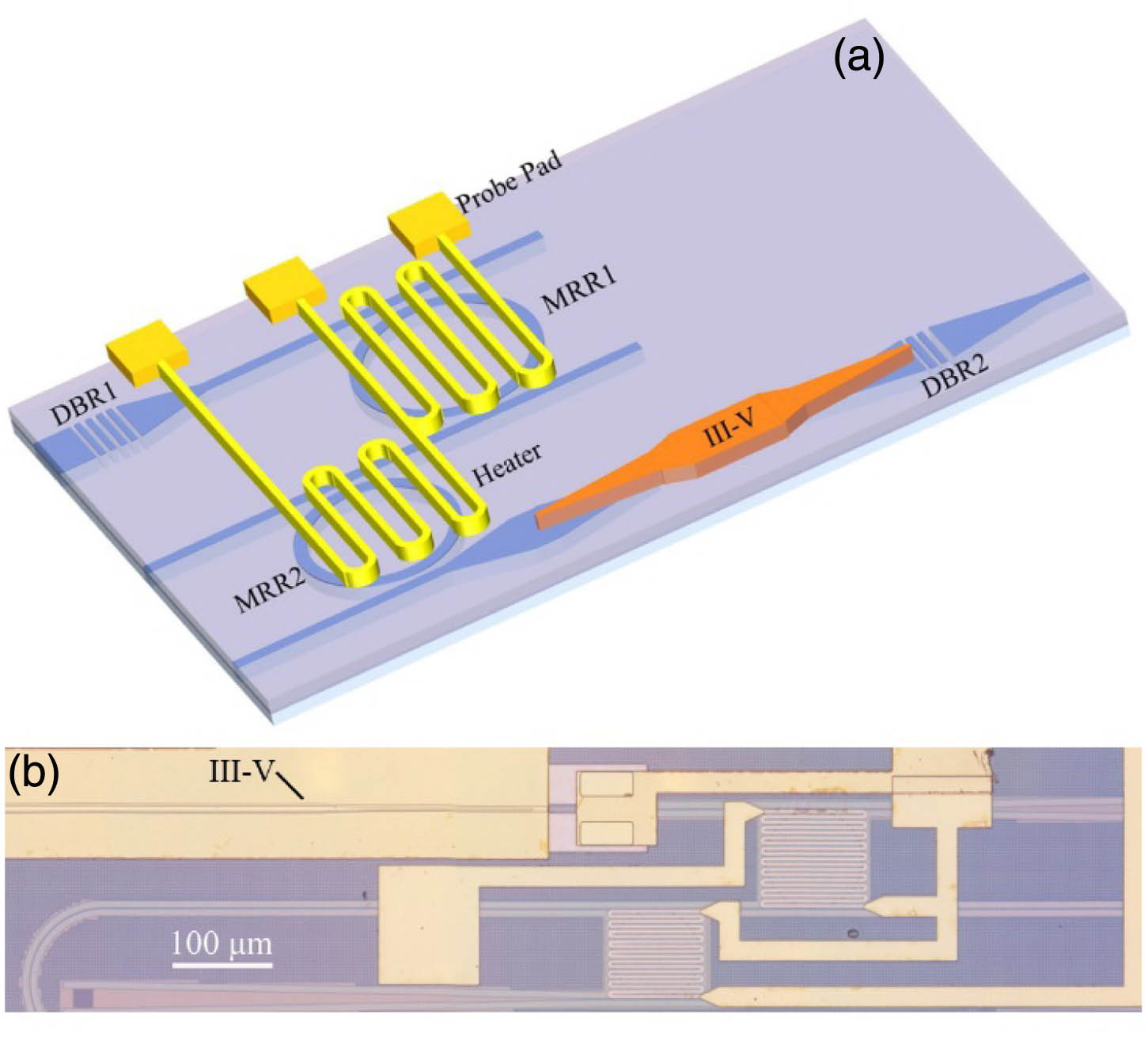
Figure 1.(a) Schematic of the widely tunable III-V-on-silicon laser; (b) microscope image of the fabricated laser.

Figure 2.(a) Simulated reflectivity of DBR1 and DBR2. The inset shows the cross section of the fabricated DBRs; (b) dependence of the reflection spectra on the pitch of DBR1; (c) simulated transmission spectra of the two MRRs and Vernier filter; (d) longitudinal modes of the Fabry–Perot cavity filtered by the Vernier filter.
A silicon Vernier filter consisting of two silicon MRRs with slightly different radii is implemented in the Fabry–Perot cavity to select the lasing wavelength. The radii of MRR1 and MRR2 are 49.1 and 44.7 μm, respectively. The different MRR radii lead to different free spectral ranges (FSRs). The corresponding FSRs of the two MRRs are 5 and 5.5 nm, respectively. Figure 2(c) shows the calculated transmission spectra of the cascaded MRRs, assuming an MRR quality factor and no waveguide loss. The transmission reaches a maximum when the resonant peaks of the two MRRs overlap. Therefore, when incorporating such a Vernier filter in the laser cavity, the lasing wavelength is determined by this alignment of MRR transmission spectra. More precisely, the laser emits at the longitudinal mode of the Fabry–Perot cavity that sees the highest transmission through the Vernier filter, as shown in Fig. 2(d). The FSR of the Vernier filter is 55 nm. In order to tune the laser wavelength, a microheater is integrated on both MRRs to thermally tune the overlapping resonant peak by the thermo-optic effect.
The silicon photonic ICs are fabricated in imec’s CMOS pilot line on a 200 mm SOI wafer with a 400 nm thick silicon device layer and a 2 μm thick buried oxide layer. 193 nm deep UV lithography is used to pattern the silicon waveguides and gratings, after which the silicon structures are etched 180 nm deep by inductively coupled plasma (ICP) dry etching. Then, is deposited on the wafer and planarized by chemical mechanical polishing (CMP) down to the silicon device layer. After silicon processing, an InP-based type-II epitaxial layer stack is adhesively bonded on the silicon photonic IC using a 50 nm thick DVS-BCB layer. Afterwards, the InP substrate is removed by hydrochloric acid wet etching. Then the III-V-on-silicon SOAs are processed in the III-V membrane. In the devices, the III-V waveguide is encapsulated with DVS-BCB for device passivation. Detailed information about the III-V processes used for realizing the heterogeneously integrated devices can be found in Ref. [32]. After III-V processing, microheaters are deposited on the DVS-BCB passivation layer. The heaters contain two levels of metal: one for the resistor and one for the electrical tracks and pads. The first metal layer is a high-resistivity layer that consists of 100 nm of titanium and 10 nm of gold, while in the second layer, 500 nm thick gold is used. The second metal layer overlaps with the first layer except in the metal heater spiral on the MRRs. A microscope image of the III-V-on-silicon Vernier laser is shown in Fig. 1(b).
3. MEASUREMENT RESULTS
Fabricated III-V-on-silicon chips are mounted on a temperature-controlled sample stage during measurements. The light in the silicon waveguide couples to a standard single-mode fiber (SMF-28) through an integrated grating coupler. The measured chip-to-fiber coupling efficiency of the grating coupler is around at 2.35 μm, and the 3 dB bandwidth is 150 nm. The fiber is connected with an optical spectrum analyzer (OSA, Yokogawa AQ6375) for laser characterization. The OSA was used at a resolution of 0.1 nm during measurements.
A. SOA and Fabry–Perot Lasers
In the III-V-on-silicon chip, heterogeneously integrated InP-based type-II SOAs and Fabry–Perot lasers are coprocessed with Vernier lasers. The III-V-on-silicon SOA has a 1000 μm long and 3.8 μm wide gain section and is integrated on a silicon waveguide with connected grating couplers on both sides. The gain of the SOA is extracted by comparing the fiber-to-fiber transmission through a reference waveguide [black dots in the inset of Fig. 3(a)] and the waveguide with integrated III-V SOA [red dots in the inset of Fig. 3(a)]. The extracted gain spectrum of the amplifier at 150 mA bias at 5°C is shown in Fig. 3(a). The maximum on-chip gain is 9.5 dB at 2340 nm. The 1 dB bandwidth of the gain spectrum is 60 nm (2310–2370 nm) and the 3 dB bandwidth is fitted to be 120 nm (2280–2400 nm). This broadband gain spectrum matches our previous DFB laser array results [22] and enables a widely tunable laser source based on this III-V-on-silicon optical amplifier. By integrating two silicon DBRs (DBR1 and DBR2) with the III-V-on-silicon SOA, a Fabry–Perot laser is realized. Figures 3(b)–3(d) show the emission spectra of three Fabry–Perot lasers with different DBR pitches under the same bias condition. The lasing spectra are quite different, which is related to the different reflection spectra of DBR1, as shown in Fig. 2(b). For the laser with a DBR pitch of 420 nm, a notch in the emission spectrum can be observed around 2360 nm, which is attributed to a notch in the reflectivity on the red side of the DBR stopband at that wavelength. The laser with 460 nm DBR pitch shows a similar notch at 2310 nm, as marked in Fig. 3(d), corresponding to the notch on the blue side of the DBR stopband. A blueshift can be found by comparing the simulated reflection spectra and lasing spectra, which can be ascribed to the nonideal vertical profile of the fabricated silicon gratings, as shown in the inset of Fig. 2(a).
Figure 3.(a) Gain spectrum of the III-V-on-silicon SOA at 150 mA at 5°C. The inset shows the fiber-to-fiber transmission spectra of the silicon waveguide with (in red) and without (in black) integrated SOA. (b)–(d) Emission spectra from III-V-on-silicon Fabry–Perot lasers with different DBR pitches. All Fabry–Perot lasers are driven at 160 mA at 5°C in CW regime.
B. III-V-on-Silicon Vernier Lasers
Figure 4(a) shows the on-chip light-current (L-I) characteristic of a III-V-on-silicon Vernier laser with a DBR pitch of 420 nm and MRR quality factor of 1500 under continuous wave (CW) operation at different temperatures. In the L-I measurements, the device is lasing at approximately 2340 nm. The threshold current is 85 mA at 0°C and increases to 125 mA at 10°C. For a laser with a 900 μm long and 5 μm wide gain section, these threshold current values correspond to a current density of at 0°C and at 10°C. The maximum on-chip output power is 1.4 mW at 0°C and reduces to 0.4 mW at 10°C. The kinks in the L-I curve result from mode hopping in the Fabry–Perot cavity and will be discussed later. A high-resolution emission spectrum of the laser biased at 150 mA at 5°C is shown in Fig. 4(b). Single-mode lasing with a side-mode suppression ratio (SMSR) of 49 dB is achieved. The main side mode in the lasing spectrum results from the resonances next to the overlapping resonant peak shown in Fig. 2(c). Besides, in CW regime, the laser is also characterized in a pulsed mode (pulse duration 1 μs, period of 100 μs). Under pulsed operation, the laser outputs a peak power of 3.5 mW at 5°C and 1 mW at 25°C. The maximun operating temperature of the III-V-on-silicon laser can be improved by further optimizing the InP-based type-II epitaxial layer structure to enhance the carrier injection efficiency [37]. Besides, reducing the thickness of buried oxide or connecting the top heat spreader to the silicon substrate can reduce the thermal impedance and improve the maximum operating temperature.
Figure 4.(a) CW L-I curve of the III-V-on-silicon Vernier laser with 420 nm DBR and MRRs with quality factor of 1500; (b) a fiber-coupled emission spectrum of the Vernier laser.
For the Vernier laser, the SMSR can be improved by using MRRs with a higher Q factor. By varying the coupling length and gap between the MRR and the bus waveguide, the Q factor of the MRR can be changed. In this work, we studied III-V-on-silicon Vernier lasers with measured MRR Q factors around 500, 1500, 2500, and 5000. Figures 5(a) and 5(b) show a typical emission spectrum from the Vernier laser with the lowest Q and highest Q MRR, respectively. The longitudinal modes of the Fabry–Perot cavity can be clearly seen from the lasing spectrum of the laser with the lowest Q MRR. The SMSR is only 38 dB for this laser. When the Q factor increases to 5000, only one mode can be seen in the lasing spectrum, as shown in Fig. 5(b). In this case, the SMSR improves to 53 dB. However, the higher Q factor also introduces higher loss in the laser cavity, which results in higher threshold current and lower output power. When the Q factor increases from 500 to 5000, the threshold current increases from 78 to 130 mA and the maximum on-chip output power decreases from 1.6 to 0.8 mW at 0°C.
Figure 5.Fiber-coupled emission spectrum of the laser with different MRRs. (a) , biased at 160 mA at 5°C; (b) , biased at 160 mA at 0°C.
The lasing wavelength of the Vernier lasers is tuned by thermally adjusting the position of the overlapping resonant peak of the two MRRs using integrated microheaters. Figures 6(a)–6(c) show CW superimposed lasing spectra and output power (indicated by the stars) of lasers with different DBR pitches when driven at 160 mA. A CW tuning range of 30 nm is achieved for the laser with DBR pitch of 435 nm. The tuning is realized by varying the electrical power dissipated in the microheater on top of MRR2. The wavelength spacing in the tuning is determined by the FSR of the unheated MRR. In the measurements, change in the heater power dissipation leads to the change in the lasing wavelength, as shown in Fig. 6(d). From these figures, it can be seen that lasers with different DBR pitches are operating in different spectral ranges. The laser with DBR pitch of 420 nm is tuned from 2322 to 2347 nm. When the DBR pitch increases to 460 nm, the tuning range also shifts to 2337–2362 nm. These tuning ranges match the lasing spectra of Fabry–Perot lasers with the same DBR pitch shown in Figs. 2(b) and 2(c). The dependence of output power on lasing wavelength matches the gain spectrum of the III-V-on-silicon SOA.
Figure 6.Superimposed CW lasing spectra of lasers with (a) DBR pitch of 420 nm and MRR Q factor of 2500, (b) DBR pitch of 435 nm and MRR Q factor of 2500, and (c) DBR pitch of 460 nm and MRR Q factor of 1500. All lasers are biased at 160 mA, the two lasers with the higher Q MRRs are measured at 0°C, and the laser with lower Q is measured at 5°C. (d) Dependence of the lasing wavelength on the electrical power dissipated in the two MRRs of the laser shown in (b).
In the III-V-on-silicon Vernier lasers discussed above, the DVS-BCB spacer between the silicon MRRs and the resistive heaters is around 1.8 μm thick. Because DVS-BCB is a low thermal conductivity material, reducing the DVS-BCB gap can improve the thermal tuning efficiency, which enables a wider tuning range for a given maximum affordable power dissipation in the heaters. Therefore, we also processed another sample with 1 μm DVS-BCB gap to get a wider tuning range. However, the lasers with MRRs Q factor of 1500 cannot lase in CW at 5°C when the DVS-BCB gap reduces to 1 μm. The laser only lases when the microheaters are removed from the top of the MRRs. This phenomenon indicates that the smaller spacing introduces extra loss into the laser cavity, since the overlap between the mode in the silicon and the metal heater spiral becomes stronger. Figure 7 shows the superimposed lasing spectra of two Vernier lasers with 1 μm BCB gap in the pulsed regime (pulse duration 1 μs, period of 100 μs), for which higher peak gain is available. During measurements, both lasers are driven at 150 mA peak current at 5°C. A 5 nm wavelength tuning requires a change in the heater power dissipation. The laser with DBR pitch of 420 nm can be tuned around 40 nm centered at 2320 nm. When the DBR pitch increases to 460 nm, the laser can cover near 50 nm tuning range centered at 2350 nm. By on-chip combining of the two lasers with different DBRs, a wavelength tuning over 70 nm can be achieved. These pulsed tunable laser sources also can be used in trace gas measurements [38,39]. To achieve such a wide wavelength tuning range in CW operation, the DVS-BCB passivation layer can be replaced by, e.g., silicon nitride, which has higher thermal conductivity. In this case, the metal spiral heater and silicon waveguides are optically separated while keeping an efficient thermal tuning.
Figure 7.Superimposed lasing spectra (pulsed) of lasers with (a) DBR pitch of 420 nm and MRR Q factor of 2500 and (b) DBR pitch of 460 nm and MRR Q factor of 1500. Both lasers are driven at 150 mA at 5°C.
When the Vernier laser is tuned by heating one of the MRRs, the tuning resolution is limited by the FSR of the unheated MRR. In order to achieve a fine wavelength tuning, both MRRs should be simultaneously heated. Figure 8 shows a wavelength tuning with a resolution of 0.3 nm over a range of about 2 nm by simultaneously tuning two heaters. Based on this tuning method, the lasing wavelength can be precisely moved close to gas absorption lines. The tuning resolution by heating two MRRs is still limited by the longitudinal mode spacing of the Fabry–Perot cavity. The overall Fabry–Perot cavity length is 2.2 mm, which corresponds to a longitudinal mode spacing of around 0.3 nm. To continuously tune over 0.3 nm, integrating a phase section in the laser cavity is a possible solution [33]. Here we continuously tune the lasing wavelength by adjusting the bias current. In this method, the increase of bias current results in a temperature increase of the gain section, which leads to an increase in the refractive index of the III-V waveguide and effective laser cavity length. Therefore, the lasing wavelength can be continuously tuned by varying the bias current. A contour map of the fiber-coupled laser spectra as a function of the bias current at 5°C is shown in Fig. 9, for a Vernier laser with MRR Q factor of 1500. This spectral map corresponds to the L-I curve shown in Fig. 4(a). It can be clearly seen that a 30 mA change in the bias current leads to a shift in the lasing wavelength. When the lasing mode is tuned too far from the overlapping resonant peak of the two MRRs, the laser will hop to another longitudinal mode closer to the transmission peak of the Vernier filter. Since the FSR of the longitudinal mode is around 0.3 nm, the laser keeps lasing in the 0.3 nm spectral range centered at the overlapping resonant peak, as seen in Fig. 9.
Figure 8.Superimposed CW lasing spectra obtained by tuning both MRRs.
Figure 9.Spectral map of fiber-coupled emission spectrum of a Vernier laser as a function of bias current at 5°C in CW regime.
C. TDLAS Measurement
In order to verify the performance of the III-V-on-silicon Vernier laser in TDLAS, a direct absorption spectroscopy experiment of CO gas is carried out. A Vernier laser with DBR pitch of 420 nm and MRR Q factor of 1500 is used as the laser source. The light from the laser is coupled to an SMF through the on-chip grating coupler, and then coupled to a CO gas cell using a collimator and two adjustable plane mirrors. After interaction with the CO, the light is coupled to a Yokogawa OSA or a photodetector through a collimator. The 10 cm long gas cell contains pure CO gas at a pressure of 740 Torr and is antireflection-coated for 2.3 μm wavelength to achieve an efficient optical coupling. The total insertion loss of the TDLAS setup is around 15 dB. During TDLAS measurements, the laser is operated at 5°C in CW regime. By adjusting the thermal power dissipated in the heaters on top of the two MRRs, the laser emission wavelength is moved close to the absorption lines of CO. Then high-resolution spectroscopy is achieved by continuously tuning the laser bias current. The maximum absorption occurs around 2332 nm wavelength. In the measurements, we tune the Vernier laser to a few absorption lines with different line intensity, including the strongest one. Figure 10(a) shows the contour map of the fiber-coupled laser spectrum near the 2337 nm wavelength after interaction with the gas. Three absorption dips can be seen in the spectral map as the bias current increases from 120 to 200 mA. The strong absorption happens when the lasing wavelength is at 2337.4 nm. Based on the current-wavelength relationship, three measured TDLAS spectra and corresponding high-resolution transmission molecular absorption (HITRAN) spectra are shown in Figs. 10(b)–10(d). In the measurements, the bias current is increased with a step of 0.5 mA [Fig. 10(b)] or 1 mA [Figs. 10(c) and 10(d)], which corresponds to a wavelength step of 5 or 10 pm. The measured absorption dip and 3 dB bandwidth match very well to the reference HITRAN data for all three absorption lines. These measurement results indicate that the performance of the III-V-on-silicon Vernier laser is suitable for TDLAS measurement of gases. As the absorption windows of many gases (e.g., , , CO, and HF) overlap with the wavelength tuning range, such a laser source has great potential for multispecies trace gas spectroscopy.
Figure 10.(a) Contour map of the fiber-coupled laser spectra after the light has passed through the CO gas cell; (b)–(d) TDLAS spectrum of CO gas and the corresponding HITRAN spectrum at different absorption lines. The driven current used in the TDLAS measurements is shown in the respective figures.
4. CONCLUSION
We have presented widely tunable III-V-on-silicon Vernier lasers operating near the 2.35 μm wavelength. An InP-based type-II SOA is heterogeneously integrated on a silicon waveguide circuit providing wavelength-selective optical feedback. The SOA exhibits an on-chip gain of 9.5 dB with a 3 dB bandwidth of centered at 2.34 μm at 5°C. In the silicon waveguide circuit, a Fabry–Perot laser cavity is formed between two silicon DBRs, while a Vernier filter consisting of two silicon MRRs is integrated in the cavity to select the lasing wavelength. The Vernier lasers can provide a single-mode tuning range over 25 nm in the CW regime and in the pulsed regime at 5°C. We have studied lasers with MRRs with different Q factors. MRRs with a Q factor of 1500 can ensure the laser tunes smoothly and has an SMSR better than 40 dB over the whole tuning range in CW operation. High-Q MRRs lead to higher SMSR but also result in higher threshold current and lower output power. Vernier lasers with different DBR grating pitches are also studied in this paper, since the different DBR pitches can address different parts of the gain spectrum of the III-V-on-silicon SOA. By combining two lasers with different pitches, a wavelength tuning coverage of over 70 nm is achieved. Continuous tuning over 0.3 nm by varying the bias current allows the measurement of sharp gas absorption lines, enabling multispecies trace gas detection.
Acknowledgment
Acknowledgment. The authors would like to thank S. Verstuyft and M. Muneeb for metallization processing help.
References
[1] L. S. Rothman, I. E. Gordon, Y. Babikov, A. Barbe, D. Chris Benner, P. F. Bernath, M. Birk, L. Bizzocchi, V. Boudon, L. R. Brown, A. Campargue, K. Chance, E. A. Cohen, L. H. Coudert, V. M. Devi, B. J. Drouin, A. Fayt, J.-M. Flaud, R. R. Gamache, J. J. Harrison, J.-M. Hartmann, C. Hill, J. T. Hodges, D. Jacquemart, A. Jolly, J. Lamouroux, R. J. Le Roy, G. Li, D. A. Long, O. M. Lyulin, C. J. Mackie, S. T. Massie, S. Mikhailenko, H. S. P. Müller, O. V. Naumenko, A. V. Nikitin, J. Orphal, V. Perevalov, A. Perrin, E. R. Polovtseva, C. Richard, M. A. H. Smith, E. Starikova, K. Sung, S. Tashkun, J. Tennyson, G. C. Toon, V. G. Tyuterev, G. Wagner. The HITRAN2012 molecular spectroscopic database. J. Quant. Spectrosc. Radiat. Transfer, 130, 4-50(2013).
[2] N. V. Alexeeva, M. A. Arnold. Near-infrared microspectroscopic analysis of rat skin tissue heterogeneity in relation to noninvasive glucose sensing. J. Diabetes Sci. Technol., 3, 219-232(2009).
[3] J. Hodgkinson, R. P. Tatam. Optical gas sensing: a review. Meas. Sci. Technol., 24, 012004(2013).
[4] M. W. Sigrist, R. Bartlome, D. Marinov, J. M. Rey, D. E. Vogler, H. Wächter. Trace gas monitoring with infrared laser-based detection schemes. Appl. Phys. B, 90, 289-300(2008).
[5] A. Elia, P. M. Lugarà, C. Di Franco, V. Spagnolo. Photoacoustic techniques for trace gas sensing based on semiconductor laser sources. Sensors, 9, 9616-9628(2009).
[6] A. Hangauer, J. Chen, R. Strzoda, M. Ortsiefer, M.-C. Amann. Wavelength modulation spectroscopy with a widely tunable InP-based 2.3 micron vertical-cavity surface-emitting laser. Opt. Lett., 33, 1566-1568(2008).
[7] B. Gerhard, A. Bachmann, J. Rosskopf, M. Ortsiefer, J. Chen, A. Hangauer, R. Meyer, R. Strzoda, M.-C. Amann. Comparison of InP-and GaSb-based VCSELs emitting at 2.3 μm suitable for carbon monoxide detection. J. Cryst. Growth, 323, 442-445(2011).
[8] J. Chen, A. Hangauer, R. Strzoda, M. C. Amann. VCSEL-based calibration-free carbon monoxide sensor at 2.3 μm with in-line reference cell. Appl. Phys. B, 102, 381-389(2011).
[9] X. Chao, J. B. Jeffries, R. K. Hanson. Absorption sensor for CO in combustion gases using 2.3 μm tunable diode lasers. Meas. Sci. Technol., 20, 115201(2009).
[10] F. Stritzke, O. Diemel, S. Wagner. TDLAS-based NH3 mole fraction measurement for exhaust diagnostics during selective catalytic reduction using a fiber-coupled 2.2-μm DFB diode laser. Appl. Phys. B, 119, 143-152(2015).
[11] Vertilas GmbH. Sensing applications.
[12] Nanoplus GmbH. Distributed feedback lasers.
[13] B. L. Upschulte, D. M. Sonnenfroh, M. G. Allen. Measurements of CO, CO2, OH, and H2O in room temperature and combustion gases by use of a broadly current-tuned multi-section InGaAsP diode laser. Appl. Opt., 38, 1506-1512(1999).
[14] D. Weidmann, A. A. Kosterev, F. K. Tittel, N. Ryan, D. McDonald. Application of a widely electrically tunable diode laser to chemical gas sensing with quartz-enhanced photoacoustic spectroscopy. Opt. Lett., 29, 1837-1839(2004).
[15] G. Wysocki, R. Lewicki, R. F. Curl, F. K. Tittel, L. Diehl, F. Capasso, M. Troccoli, G. Hofler, D. Bour, S. Corzine, R. Maulini, M. Giovannini, J. Faist. Widely tunable mode-hop free external cavity quantum cascade lasers for high resolution spectroscopy and chemical sensing. Appl. Phys. B, 92, 305-311(2008).
[16] M. von Edlinger, R. Weih, J. Scheuermann, L. Nähle, M. Fischer, J. Koeth, M. Kamp, S. Höfling. Monolithic single mode interband cascade lasers with wide wavelength tunability. Appl. Phys. Lett., 109, 201109(2016).
[17] S. Kalchmair, R. Blanchard, T. S. Mansuripur, G.-M. de Naurois, C. Pfluegl, M. F. Witinski, L. Diehl, F. Capasso, M. Loncar. High tuning stability of sampled grating quantum cascade lasers. Opt. Express, 23, 15734-15747(2015).
[18] K. Vizbaras, E. Dvinelis, I. Šimonytė, A. Trinkūnas, M. Greibus, R. Songaila, T. Žukauskas, M. Kaušylas, A. Vizbaras. High power continuous-wave GaSb-based superluminescent diodes as gain chips for widely tunable laser spectroscopy in the 1.95–2.45 μm wavelength range. Appl. Phys. Lett., 107, 011103(2015).
[19] S. Latkowski, A. Hänsel, P. J. van Veldhoven, D. D’Agostino, H. Rabbani-Haghighi, B. Docter, N. Bhattacharya, P. J. A. Thijs, H. P. M. M. Ambrosius, M. K. Smit, K. A. Williams, E. A. J. M. Bente. Monolithically integrated widely tunable laser source operating at 2 μm. Optica, 3, 1412-1417(2016).
[20] A. Spott, J. Peters, M. L. Davenport, E. J. Stanton, C. D. Merritt, W. W. Bewley, I. Vurgaftman, C. S. Kim, J. R. Meyer, J. Kirch, L. J. Mawst, D. Botez, J. E. Bowers. Quantum cascade laser on silicon. Optica, 3, 545-551(2016).
[21] W. Zhou, D. Wu, R. McClintock, S. Slivken, M. Razeghi. High performance monolithic, broadly tunable mid-infrared quantum cascade lasers. Optica, 4, 1228-1231(2017).
[22] R. Wang, S. Sprengel, G. Boehm, R. Baets, M.-C. Amann, G. Roelkens. Broad wavelength coverage 2.3 μm III-V-on-silicon DFB laser array. Optica, 4, 972-975(2017).
[23] E. J. Stanton, A. Spott, N. Volet, M. L. Davenport, J. E. Bowers. High-brightness lasers on silicon by beam combining. Proc. SPIE, 10108, 101080K(2017).
[24] L. Vivien, L. Pavesi. Handbook of Silicon Photonics(2016).
[25] Y. Zou, S. Chakravarty, C.-J. Chung, X. Xu, R. T. Chen. Mid-infrared silicon photonic waveguides and devices. Photon. Res., 6, 254-276(2018).
[26] H. Lin, Z. Luo, T. Gu, L. C. Kimerling, K. Wada, A. Agarwal, J. Hu. Mid-infrared integrated photonics on silicon: a perspective. Nanophotonics, 7, 393-420(2017).
[27] L. Tombez, E. J. Zhang, J. S. Orcutt, S. Kamlapurkar, W. M. J. Green. Methane absorption spectroscopy on a silicon photonic chip. Optica, 4, 1322-1325(2017).
[28] E. M. P. Ryckeboer, R. Bockstaele, M. Vanslembrouck, R. Baets. Glucose sensing by waveguide-based absorption spectroscopy on a silicon chip. Biomed. Opt. Express, 5, 1636-1648(2014).
[29] J. T. Robinson, L. Chen, M. Lipson. On-chip gas detection in silicon optical microcavities. Opt. Express, 16, 4296-4301(2008).
[30] N. Hattasan, B. Kuyken, F. Leo, E. Ryckeboer, D. Vermeulen, G. Roelkens. High-efficiency SOI fiber-to-chip grating couplers and low-loss waveguides for the short-wave infrared. IEEE Photon. Technol. Lett., 24, 1536-1538(2012).
[31] A. Spott, M. Davenport, J. Peters, J. Bovington, M. J. R. Heck, E. J. Stanton, I. Vurgaftman, J. Meyer, J. Bowers. Heterogeneously integrated 2.0 μm CW hybrid silicon lasers at room temperature. Opt. Lett., 40, 1480-1483(2015).
[32] R. Wang, S. Sprengel, G. Boehm, M. Muneeb, R. Baets, M. C. Amann, G. Roelkens. 2.3 μm range InP-based type-II quantum well Fabry-Perot lasers heterogeneously integrated on a silicon photonic integrated circuit. Opt. Express, 24, 21081-21089(2016).
[33] R. Wang, A. Malik, I. Šimonytė, A. Vizbaras, K. Vizbaras, G. Roelkens. Compact GaSb/silicon-on-insulator 2.0× μm widely tunable external cavity lasers. Opt. Express, 24, 28977-28986(2016).
[34] G. Roelkens, A. Abbasi, P. Cardile, U. Dave, A. De Groote, Y. de Koninck, S. Dhoore, X. Fu, A. Gassenq, N. Hattasan, Q. Huang, S. Kumari, S. Keyvaninia, B. Kuyken, L. Li, P. Mechet, M. Muneeb, D. Sanchez, H. Shao, T. Spuesens, A. Subramanian, S. Uvin, M. Tassaert, K. Van Gasse, J. Verbist, R. Wang, Z. Wang, J. Van Campenhout, X. Yin, J. Bauwelinck, G. Morthier, R. Baets, D. Van Thourhout. III-V-on-silicon photonic devices for optical communication and sensing. Photonics, 2, 969-1004(2015).
[35] A. Spott, E. J. Stanton, N. Volet, J. D. Peters, J. R. Meyer, J. E. Bowers. Heterogeneous integration for mid-infrared silicon photonics. IEEE J. Sel. Top. Quantum Electron., 23, 8200810(2017).
[36] R. Wang, M. Muneeb, S. Sprengel, G. Boehm, A. Malik, R. Baets, M.-C. Amann, G. Roelkens. III-V-on-silicon 2-μm-wavelength-range wavelength demultiplexers with heterogeneously integrated InP-based type-II photodetectors. Opt. Express, 24, 8480-8490(2016).
[37] S. Sprengel, C. Grasse, P. Wiecha, A. Andrejew, T. Gruendl, G. Boehm, R. Meyer, M.-C. Amann. InP-based type-II quantum-well lasers and LEDs. IEEE J. Sel. Top. Quantum Electron., 19, 1900909(2013).
[38] G. Wysocki, M. McCurdy, S. So, D. Weidmann, C. Roller, R. F. Curl, F. K. Tittel. Pulsed quantum-cascade laser-based sensor for trace-gas detection of carbonyl sulfide. Appl. Opt., 43, 6040-6046(2004).
[39] J. Jágerská, P. Jouy, B. Tuzson, H. Looser, M. Mangold, P. Soltic, A. Hugi, R. Brönnimann, J. Faist, L. Emmenegger. Simultaneous measurement of NO and NO2 by dual-wavelength quantum cascade laser spectroscopy. Opt. Express, 23, 1512-1522(2015).

