
Tianyu Liu, Peng Ran, Yirong Su, Zeng Chen, Renchen Lai, Weidong Shen, Yaoguang Ma, Haiming Zhu, Yang (Michael) Yang. Solution-processed halide perovskite microcavity exciton-polariton light-emitting diodes working at room temperature[J]. Photonics Research, 2023, 11(10): 1791
- Photonics Research
- Vol. 11, Issue 10, 1791 (2023)
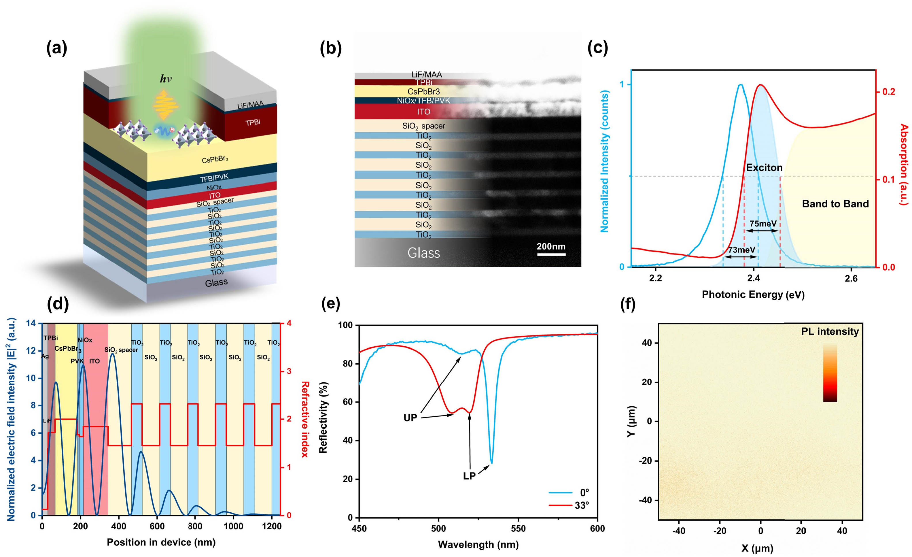
Fig. 1. Structure of the device and basic properties. (a) Schematic structure architecture; (b) cross section scanning electron microscope (SEM) image of the device; (c) normalized emission (blue) and absorption (red) of prepared CsPbBr 3 100 μm × 100 μm

Fig. 2. Angle-resolved reflectivity and analysis. (a) Angle-resolved reflectivity (black lines) of devices at three different normal cavity–exciton detunings: Δ = 1.1 − 77 − 128 meV
Fig. 3. Optoelectronic performance of the device. (a)–(c) Angle-resolved PL/EL spectra of the three detunings. UPs, LPs, E x E ph 2 are marked simultaneously. (d) Energy-level diagram of the as-fabricated device; (e), (f) comparison of current density(J )-voltage(V )-luminance(L )-external quantum efficiency (EQE) curves (inset: photograph of perovskite exciton–polariton LED at operation); (g) spectral stability of the − 77 meV − 77 meV − 77 meV 700 cd / cm 2
Fig. 4. Influence of MAA electrode thickness on device performance. (a) Angle-resolved reflectivity of devices with 20 and 40 nm MAA as top electrodes; (b), (c) angle-resolved PL/EL of devices with 20 and 40 nm MAA as top electrodes; (d), (e) J-V-L -EQE characteristics; (f) normal EL spectra with 20 and 40 nm MAA electrodes.
Fig. 5. Fabrication process of our perovskite polariton LED.
Fig. 6. Schematic diagram of normal reflection detection.
Fig. 7. Additional reliability data of device fabrication. (a) Reflection of TiO 2 / SiO 2 CsPbBr 3 CsPbBr 3 CsPbBr 3 CsPbBr 3 I ( T ) = I 0 / ( 1 + A ⋅ exp ( − E b / KT ) ) E b x y
Fig. 8. (a), (b) J-V-L -EQE characteristics of reference LED without microcavity. (c) Current density versus voltage curves of hole-only and electron-only devices.
Fig. 9. (a) Simulation of bare cavity reflectivity. The FWHM of cavity mode is 36 meV. (b) Comparison of simulated reflection of bare cavity with 20 and 40 nm MAA top electrode. (c) Simulated reflection of cavity mode with thickness of MAA from 10 to 50 nm.

Set citation alerts for the article
Please enter your email address
© Copyright 2018-2021 | Chinese Laser Press. All Rights Reserved 沪ICP备15018463号-20