• Chinese Optics Letters
  • Vol. 15, Issue 8, 081301 (2017)
Minyue Yang, Mingyu Li, and Jianjun He*
Author Affiliations
  • State Key Laboratory of Modern Optical Instrumentation, Centre for Integrated Optoelectronics, College of Optical Science and Engineering, Zhejiang University, Hangzhou 310027, China
  • show less
    DOI: 10.3788/COL201715.081301 Cite this Article Set citation alerts
    Minyue Yang, Mingyu Li, Jianjun He. Polarization insensitive arrayed-input spectrometer chip based on silicon-on-insulator echelle grating[J]. Chinese Optics Letters, 2017, 15(8): 081301 Copy Citation Text show less
    Schematic diagram of the imaging spectrometer, where the arrayed-input EDG is used. Lens 1 represents the fore-optic lens, and the micro-electromechanical system (MEMS) mirror array operates as an optical switch array for N pixels. The chip structure is enlarged, and the arrayed input waveguides receive the N corresponding pixels one by one. Thus, the spectrum of each pixel is obtained in a time division multiplexing fashion.
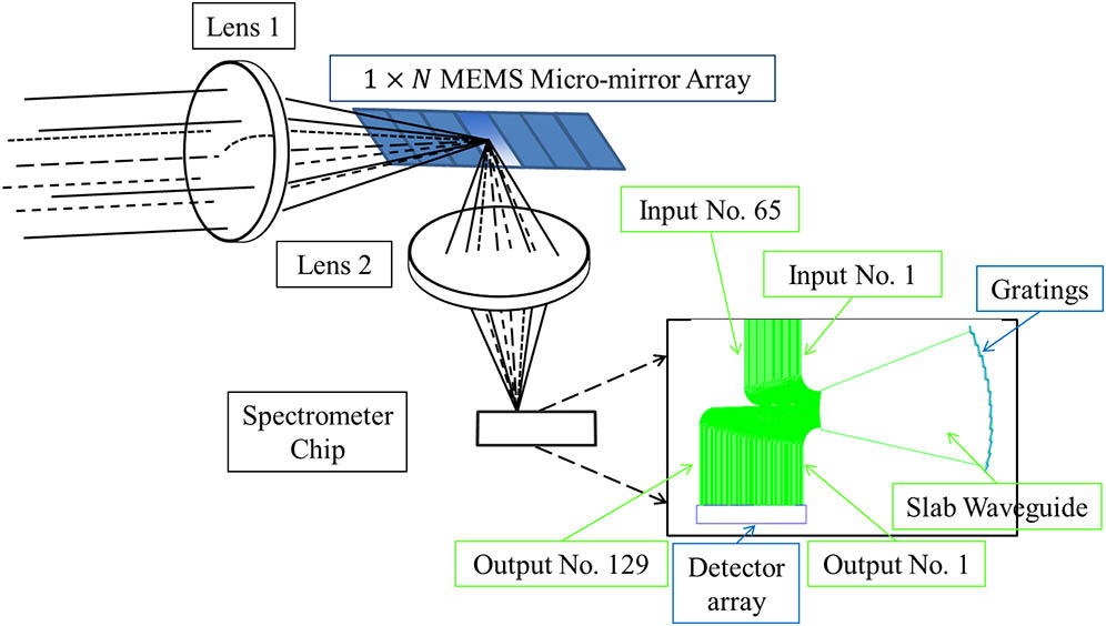
    Fig. 1. Schematic diagram of the imaging spectrometer, where the arrayed-input EDG is used. Lens 1 represents the fore-optic lens, and the micro-electromechanical system (MEMS) mirror array operates as an optical switch array for N pixels. The chip structure is enlarged, and the arrayed input waveguides receive the N corresponding pixels one by one. Thus, the spectrum of each pixel is obtained in a time division multiplexing fashion.
    (a) Scanning electron microscope (SEM) images of the cross-section of a deep etched strip waveguide, (b) cross-section of a shallow etched ridge waveguide, (c) tapers between ridge waveguides and deep etched strip waveguides, (d) cross-section of the Al coated surface, and (e) the grating facets of the EDG. (f) The photograph of the EDG chip compared with one yuan coin.
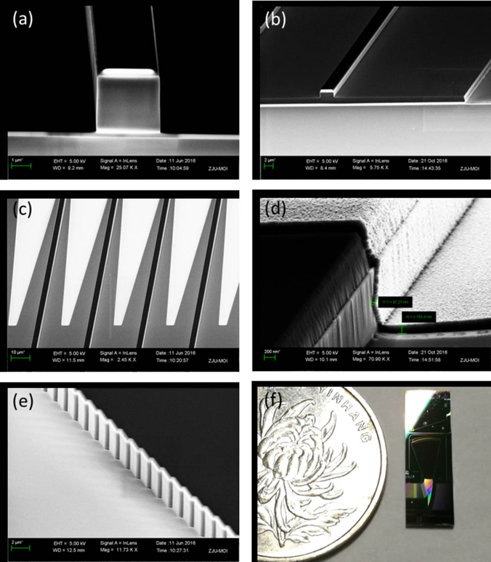
    Fig. 2. (a) Scanning electron microscope (SEM) images of the cross-section of a deep etched strip waveguide, (b) cross-section of a shallow etched ridge waveguide, (c) tapers between ridge waveguides and deep etched strip waveguides, (d) cross-section of the Al coated surface, and (e) the grating facets of the EDG. (f) The photograph of the EDG chip compared with one yuan coin.
    (Color online) Transmission spectra for (a) input waveguide No. 1, (b) input waveguide No. 33, and (c) input waveguide No. 65. The enlarged spectra for output channel Nos. 32 to 34 of input waveguide No. 33 are given in (d), showing the detailed polarization insensitive characteristics.
    Fig. 3. (Color online) Transmission spectra for (a) input waveguide No. 1, (b) input waveguide No. 33, and (c) input waveguide No. 65. The enlarged spectra for output channel Nos. 32 to 34 of input waveguide No. 33 are given in (d), showing the detailed polarization insensitive characteristics.
    Wavelength range1250–1750 nm
    Wavelength spacing of adjacent channels7.81 nm
    Linear dispersion640
    Output waveguide number129
    Input angle range5.90°–9.39°
    Output angle range1.17°5.75°
    Diffraction order m2
    Rowland circle radius r2651 μm
    Grating period d5.00 μm
    ng/neff1.047
    Table 1. Design Parameters of the EDG
    Minyue Yang, Mingyu Li, Jianjun He. Polarization insensitive arrayed-input spectrometer chip based on silicon-on-insulator echelle grating[J]. Chinese Optics Letters, 2017, 15(8): 081301
    Download Citation