State Key Laboratory of Modern Optical Instrumentation, Centre for Integrated Optoelectronics, College of Optical Science and Engineering, Zhejiang University, Hangzhou 310027, China
We demonstrate a polarization insensitive arrayed-input spectrometer using echelle diffraction grating (EDG) for hyperspectral imaging. The EDG consists of 65 input waveguides and 129 output waveguides, allowing spectral measurements of 65 image pixels at a time when used in combination with a micro-electromechanical system micro mirror array. The spectral resolution reaches 7.8 nm for wavelengths ranging from 1250 to 1700 nm. The measured loss is , and the crosstalk is lower than . The 3 μm silicon-on-insulator platform provides the device with polarization insensitive characteristics. The chip size is only .
Imaging spectrometers are most commonly used on satellites and aircrafts, including unmanned aerial vehicles (UAVs), where the spare volume and weight are limited. Recently, the development of a UAV in precision agriculture, local water quality, and forest disaster monitoring[1] calls for higher demands in the compactness of imaging spectrometers. A compact Fabry–Perot interferometer (FPI) hyperspectral imager has been reported[2]. However, the wavelength switching (by tuning the FPI air gap) takes 2 ms, which means a slow scan rate at high number of wavelength channels.
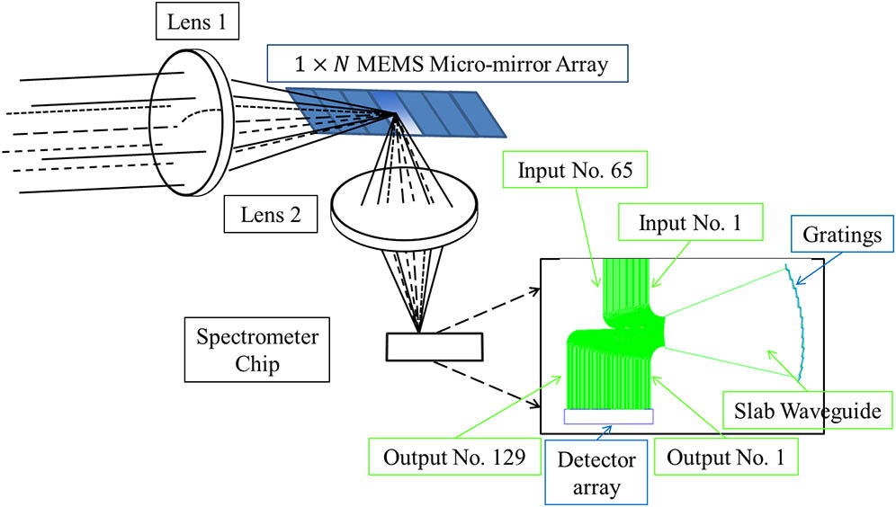
Integrated photonics have achieved great success in next-generation optical networks, optical interconnects, wavelength division multiplexing systems, coherent transceivers, and lab-on-a-chip applications[3,4]. Also, many on-chip spectrometers have been reported[5–11], including arrayed waveguide gratings (AWGs) and echelle diffraction grating (EDG) spectrometers. Due to the advantages of high resolution and multiple input waveguides along the Rowland circle in one device, we designed and experimentally demonstrated an arrayed-input EDG for a push-broom imaging spectrometer, as shown in Fig. 1, which has a small footprint and can reach a high spectral resolution and high scan rate. In this Letter, we present the design, fabrication, and experimental results of the multi-input waveguide EDG.
Figure 1.Schematic diagram of the imaging spectrometer, where the arrayed-input EDG is used. Lens 1 represents the fore-optic lens, and the micro-electromechanical system (MEMS) mirror array operates as an optical switch array for N pixels. The chip structure is enlarged, and the arrayed input waveguides receive the N corresponding pixels one by one. Thus, the spectrum of each pixel is obtained in a time division multiplexing fashion.
To achieve high optical étendue and low polarization dependence, we choose a 3 μm thick silicon-on-insulator (SOI) platform[12–14]. The numerical aperture of the silicon waveguide for the fundamental mode is 0.238 (0.2–0.275), which means that it can receive light focused from a lens of F number 2.04, smaller than the normal F number of the imaging system in the imaging spectrometer[2,15,16], so that most of the light focused from the lens can be coupled into the waveguide.
Sign up for Chinese Optics Letters TOC. Get the latest issue of Chinese Optics Letters delivered right to you!Sign up now
Figure 2.(a) Scanning electron microscope (SEM) images of the cross-section of a deep etched strip waveguide, (b) cross-section of a shallow etched ridge waveguide, (c) tapers between ridge waveguides and deep etched strip waveguides, (d) cross-section of the Al coated surface, and (e) the grating facets of the EDG. (f) The photograph of the EDG chip compared with one yuan coin.
The design of the EDG follows Rowland mounting with one stigmatic point method[17]. The input beam from one of the input waveguides on the Rowland circle radiates to the slab region and is reflected by the gratings. After being diffracted, light of different wavelengths will be focused onto different output waveguides on the Rowland circle. The grating diffraction is described by where is the effective index of the fundamental slab mode, is the grating period, and are the incident and diffraction angles, respectively, is the diffraction order, and is the wavelength in the vacuum.
Considering the imaging spectrometer application and the fabrication tolerance, we choose a wide range for the working spectrum, from 1250 to 1750 nm, with a diffraction order of 2, limited by the free spectral range (FSR) equation, where is the group index of the fundamental mode of the slab waveguide.
The structure of the slab waveguide consists of a 0.3 μm buried oxide (BOX) layer, a 3 μm silicon layer, and a 0.6 μm silicon oxide upper cladding. The effective index difference between the TE and TM modes produces a less than 0.55 nm polarization dependent wavelength shift (), according to Eq. (1), which is negligible in our case. In order to fit the device with our fabrication tolerance, we choose a 65 spectral channel device with 7.8 nm channel spacing design, meeting the hyperspectral imaging resolution requirement. The Rowland circle radius is 2651 μm. The blazed grating facets are about 5 μm long, allowing for easy fabrication and low loss caused by the corner rounding effect. The connecting facet is 0.4 μm, which is determined by the low diffraction order of the design. There are 65 input waveguides and 129 output waveguides. For the th input waveguide (), 65 output waveguides from the th to ()th will be used for collecting the spectrum of the input channel. The chip size is only , which is much smaller than the free-space grating device of traditional imaging spectrometers.
A shallow etch of 1.2 μm is used to form the single mode ridge input waveguide. It is tapered into a deep etched strip waveguide to guide the light into the slab region. Due to the fabrication requirement, the deep etched waveguides are aligned along the Rowland circle at the slab interface with a spacing of about 5 μm, forming 2 μm wide and 3 μm deep slots between the waveguides. The output angle of the 65-channel EDG is close to 0, which helps to suppress the crosstalk created by higher order modes caused by non-vertical grating facets[18,19].
The blazed angles of the gratings are adjusted to balance the loss of two edge wavelength channels, 1250 and 1750 nm, according to the Fraunhofer diffraction formula. Also as an EDG device, the blazed condition of the gratings remain for all 65 input waveguides, and the loss of all of the input waveguides is similar, which is proved by the simulation of a similar device[20].
As shown in Fig. 2, an SOI wafer with a 3 μm top silicon and a 300 nm thick BOX layer is used to fabricate the device. First, a 0.6 μm layer is deposited on to the wafer as a hard mask for silicon etching. Then, the device is patterned using AZ5214 photoresist. The pattern is transferred to the hard mask by inductivity coupled plasma (ICP). Then, all of the waveguides and gratings are etched 1.2 μm deep to form the single mode ridge input waveguides. Afterward, another photolithography step is implemented to cover the slab region of the ridge waveguides, and the exposed areas are etched to a depth of 3 μm to form the deep etched waveguides, grating facets, and tapered transitions between two types of waveguides. The side walls of the waveguides are smoothed by a thermal oxidation and wet polishing process. To increase the reflectivity of the grating facet, a 160 nm thick Al layer is coated on the back of the facets by using a photoresist-protected wet etching process.
To measure the spectral response of the device with such a wide wavelength band, we use a supercontinuum source (YSL photonics SC-5 series) and an eight-channel acousto-optic tunable filter (AOTF) tunable filter to provide light into the input waveguide via a polarization-maintaining lensed fiber. To collect the energy from the output waveguide, another lensed fiber connected to the optical spectrum analyzer (OSA, Agilent 86146B) is used. Due to the 1700 nm upper limit of the OSA, only 58 of the 65 channels could be tested. The measured spectrum is normalized with respect to the transmission spectrum of a straight waveguide to account for the coupling loss (about 7 dB) and eliminate the shape of the supercontinuum source spectrum. We measured the 58-channel spectra of the center and edge (Nos. 1, 33, and 65) input waveguides. For the No. 33 input waveguide, both the TE and TM polarizations are tested to show the polarization insensitive characteristics of the device.
As shown in Fig. 3, the insertion loss of for the multi-input EDG is mainly caused by the metal reflective coating, the corner rounding of the grating facets, and the waveguide propagation loss. The 0.2 μm radius rounding corner of the grating teeth contributes to a 1 dB loss[16], and the 90%–95% Al metal reflectivity causes about a 0.4 dB loss, which could be improved by using the lift-off process so as to replace Al with Au to get higher reflectivity. The remaining 0.6 to 2 dB loss for different output channels can be attributed to the roughness of the grating tooth and waveguide sidewalls. The channel spacing remains at 7.8 nm for all input waveguides. The center input waveguide has a channel response of 0.8 nm longer in wavelength than the two edge input waveguides, however, it is only one tenth of the device resolution, and this error can be eliminated by calibrations. Most channels of the center input waveguide (No. 33) have better crosstalk below , while for the edge input waveguides, the crosstalk is about , which is still low enough for an imaging spectrometer. The 3 dB bandwidth is 3.5 nm, which is restricted by the tolerance of the deep etching process with 3 μm wide waveguides with a 2 μm gap on the Rowland circle. The is less than 0.5 nm, and the polarization dependent loss (PDL) is less than 0.2 dB.
Figure 3.(Color online) Transmission spectra for (a) input waveguide No. 1, (b) input waveguide No. 33, and (c) input waveguide No. 65. The enlarged spectra for output channel Nos. 32 to 34 of input waveguide No. 33 are given in (d), showing the detailed polarization insensitive characteristics.
In conclusion, we demonstrate a push-broom micro-imaging spectrometer using an on-chip EDG, which is highly compact and can achieve high resolution imaging. As the first demonstration, we design and fabricate a 65 input and 129 output EDG with a 500 nm spectral range. A low on-chip loss of 2 dB and a crosstalk below are measured for all channels. This is a good performance compared to a recently reported eight-channel EDG fabricated on InP[21]. The device is polarization insensitive and has a size of only . We reduce the resolution to 7.8 nm and the channel number to 65 compared to the previous designed device in Ref. [20] because the original EDG with a 4 nm resolution is too large for us to fabricate and test. The arrayed-input EDG-based imaging spectrometer can provide a low-cost solution for high spectral resolution remote sensing with the advantages of small size, light weight, vibration proof, and high integration.
[9] I. Akca, N. Ismail, F. Sun, D. V. Nguyen, J. Kalkman, T. G. van Leeuwen, A. Driessen, K. Worhoff, M. Pollnau, R. de Ridder. Lasers and Electro-Optics IEEE, 1(2010).