Huibo Yuan, Lin Li, Te Li, Jing Zhang, Yong Wang, Zhongliang Qiao, Zhanguo Li, Yi Qu, Xiaohui Ma, Guojun Liu. Photoluminescence of a high strain InGaAs single quantum well with GaAsP barriers[J]. Chinese Optics Letters, 2015, 13(Suppl.): S21602
Copy Citation Text
To investigate the relationship between indium content and optical properties during epitaxial growth of an InGaAs/GaAs single quantum well (SQW), simulation and experiments are demonstrated. The epitaxial growth is demonstrated with low-pressure metal–organic chemical vapor deposition. Photoluminescence (PL) spectroscopy is applied to research the PL properties at room temperature. The varies from 0.24 to 0.36, resulting in an increasing of the full-width half-maximum (FWHM) with the wavelength exhibiting a red-shift. A SQW with an of 0.36 is manufactured, where a FWHM of 23.9 meV is obtained. An InGaAs SQW sandwiched by GaAsP is prepared, which is observed to exhibit a diminished FWHM of 17.0 meV with the wavelength revealing a blue-shift.
The InGaAs quantum well (QW) structure has been widely used in photoelectric devices[1,2]. Semiconductor lasers with InGaAs QW structures have been studied a lot for an effective restriction to electronics due to its narrow bandgap. Because of its lattice mismatch with GaAs substrates, moderate strain is induced to achieve a better optical performance. With epitaxial growth technology such as molecular-beam epitaxy (MBE) and metal–organic chemical vapor deposition (MOCVD), highly strained and high quality epitaxial wafers are manufactured. Low threshold current and insensitivity to temperature are observed in InGaAs/GaAs structures[3]. InGaAs/GaAs/AlGaAs QW structures grown by MOCVD at 640°C are found to exhibit a strong photoluminescence (PL) intensity with tertiarybutylarsine (TBA) as the Group V source[4]. Early work has included strain in InGaAs/GaAs QWs, but dislocations and strain accumulate with increasing In content, inducing defects and rough surfaces[5,6]. To obtain a higher output power, multiple quantum wells (MQWs) are applied[7]. Due to strain accumulation with epitaxial growth, the thickness of the epi-layer is very limited. In order to overcome the limitation of lattice mismatches and critical thickness, an InGaAs/GaAsP structure has been taken into account.
As a promising solution to lattice mismatches, GaAsP has been used as barriers instead of GaAs[2,8–10]. The bandgap of GaAsP could be nearly twice that of GaAs which results in a better restriction to electrons. The lattice constant of GaAsP is equal or smaller than that of GaAs, leading to a strain-compensated effect. Numerical simulation of InGaAs QWs with GaAs, AlGaAs, and GaAsP barriers shows that the structure with a GaAsP barrier has a moderate absorption and peak gain, which makes GaAsP the most appropriate candidate for InGaAs QWs with decent and temperature properties[1].
In this work, epitaxial growth and simulations have been carried out. PL spectroscopy is applied to characterize optical performance. A structure of InGaAs sandwiched by GaAsP barriers is grown to investigate the effect of GaAsP on PL performance.
Sign up for Chinese Optics Letters TOC. Get the latest issue of Chinese Optics Letters delivered right to you!Sign up now
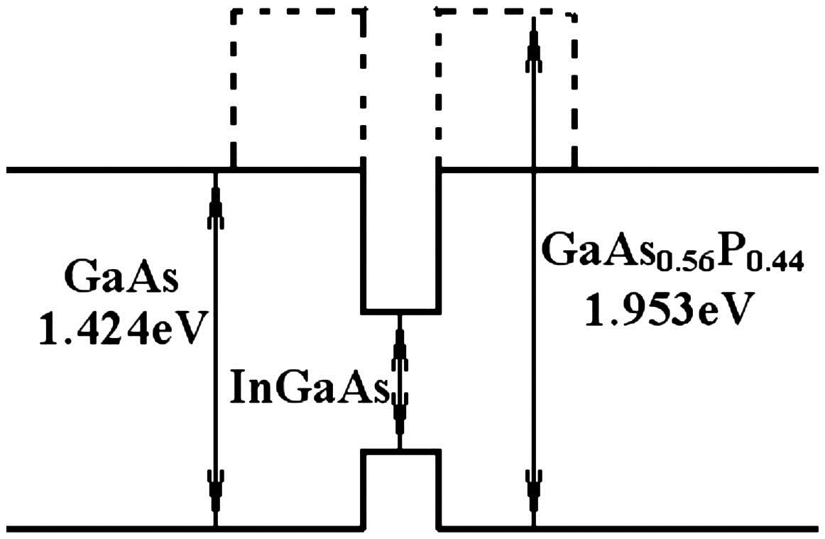
An InGaAs/GaAs single quantum well (SQW) structure is designed for epitaxial growth and simulation as schematically shown in Fig. 1. The laser technology integrated program (Lastip) has been applied for simulating.
Figure 1.Summary energy band structure of InGaAs/GaAs structure. barriers are inserted to compared to the InGaAs/GaAs SQW with a bandgap of 1.953 eV.
For , the bandgap energy can be expressed as follows[11]According to Eq. (1), the bandgap of would be 1.953 eV. There are five samples, which are Samples T1–T5. Samples T1–T4 are grown with different . Sample T5 is an InGaAs QW sandwiched by barriers with equal to T3. The material growth parameters can be seen in Table 1. The during growth and simulated In content based on wavelength measured by PL spectroscopy is shown in Table 2.
The normalized PL spectrum of different samples is shown in Fig. 2. According to Samples T1–T4, an obvious wavelength red-shift can be seen with increasing , which is from 961 to 1058.1 nm.
Figure 2.Normalized PL spectrum of Samples T1 (dash), T2 (short dash), T3 (dash dot), T4 (dash dot), and T5 (solid) with different .
As it is known, for , the bandgap energy can be expressed as follows[12]where h is Planck’s constant, is the wavelength, and is the frequency. According to Eq. (2) and (3), with In content varying from 0 to 1, decreases from 1.424 to 0.356 eV, leading to an increase in wavelength.
Based on the growth parameters of Sample T3, a SQW structure of Sample T5 with barriers between InGaAs and GaAs is manufactured. The full-width half-maximum (FWHM) of T3 and T5 are 19.5 and 17.0 meV, respectively. Both the wavelength and FWHM of Sample T5 are shorter than that of T3. The P atoms will diffuse into the QW layer due to the chemical bond energy difference between the GaAs and GaP or the conentration difference during growth[13]. The QW material will turn into an InGaAsP-like layer from InGaAs. For Sample T3, according to Table 2, the In content in the QW is 0.25 in reality, under which circumstance the bandgap energy is 1.05 eV based on Eq. (2). With the given In content value, the bandgap of can be expressed as follows With P atoms in the QW accumulating, the As content diminishes. According to Eq. (4), the bandgap of will increase with decreasing As content. Based on Eq. (3), the wavelength exhibits a diminishing effect as P atoms diffuse into the QW layer, resulting in the fact that the wavelength of T5 is shorter than T3. To prevent P diffusion or As–P exchange, the growth sequence of epilayers could be chosen to obtain a high-quality interface[13].
Figure 2 also indicates that the FWHM of Sample T5 is smaller than that of T3. The lattice constants of and can be expressed as follows According to Eq. (6) the lattice constant of is 5.75 Å. Based on Eq. (5), the lattice constant is 0.556 nm which is smaller than that of GaAs and . Tensile strain is induced during growth. With a moderate lattice constant, barriers work as strain-compensated layers, leading to a decreasing in net strain, which improves the smoothness of surfaces. As the growth quality improved, the FWHM of Sample T5 diminishes[14].
A simulation is demonstrated to compare the wavelength to the simulated results. Figure 3 reveals the relationship between the measured and simulation wavelength versus of Samples T1–T4.
Figure 3.Relationship between measured wavelength (squares) and simulation wavelength (triangles) versus of Samples T1–T4.
As shown in Fig. 3 both the simulated and measured wavelength increase with . Compared to the measured results, the simulation wavelength curve exhibits a more linear trend. There is an obvious distance between the simulation and measured wavelength curve. With increasing , the specific distance values are 53, 58.7, 82.7, and 73.4 nm, respectively. This is because there is a concentration difference of In atoms between the QW and barriers. High temperature will also provide In atoms extra kinetic energy. Due to the concentration difference and high temperature, In atoms will diffuse to other nearby layers during epitaxial growth, resulting in an insufficient usage of the trimethyl (TM) In source. Since there is a lack of In atoms, the In content in the QW becomes smaller than the heoretical values, leading to a diminishing bandgap energy. According to Eqs. (2) and (3), wavelength will increase with decreasing bandgap.
The curve in Fig. 4 reveals nearly a proportional trend. Specific FWHM values of samples can be seen in Fig. 4. A FWHM value of 23.9 meV is obtained with as high as 0.36. It can be observed from Fig. 4 that the FWHM increases with .
Figure 4.FWHM trend of Samples T1–T4 with increasing from 24 to 36.
The lattice constant of GaAs is 0.565 nm. Based on Eq. (6), the lattice constant of InGaAs increases with In content. Since the lattice constant of InGaAs is equal to or bigger than that of GaAs, compressive strain occurs during the epitaxial growth. The strain accumulates with more In contained in the QW, which induces more mismatches and defects, affecting the optical properties[15].
Experiments and simulation are demonstrated to investigate the effect of on the InGaAs SQW structure. PL spectroscopy is applied to characterize optical properties at room temperature. An enhancement of the FWHM is observed as increases, with wavelength exhibiting a red-shift. A distance between simulation and measured wavelength when the is a certain value is observed. A FWHM of 23.9 meV is obtained when the is as high as 0.36. GaAsP layers are inserted as barriers to compare to the InGaAs/GaAs structure. The FWHM is narrower than that of the structure, with the wavelength revealing a blue-shift. The structure exhibits an FWHM of 17.0 meV with a wavelength of 1014.5 nm.
Huibo Yuan, Lin Li, Te Li, Jing Zhang, Yong Wang, Zhongliang Qiao, Zhanguo Li, Yi Qu, Xiaohui Ma, Guojun Liu. Photoluminescence of a high strain InGaAs single quantum well with GaAsP barriers[J]. Chinese Optics Letters, 2015, 13(Suppl.): S21602